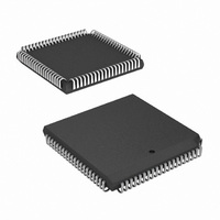
HSP50210JI-52Z Intersil, HSP50210JI-52Z Datasheet - Page 3

HSP50210JI-52Z
Manufacturer Part Number
HSP50210JI-52Z
Description
IC DEMODULATOR COSTAS 84-PLCC
Manufacturer
Intersil
Datasheet
1.HSP50210JC-52Z.pdf
(51 pages)
Specifications of HSP50210JI-52Z
Function
Demodulator
Frequency
52MHz
Rf Type
AM, FM
Package / Case
84-PLCC
Lead Free Status / RoHS Status
Lead free / RoHS Compliant
Available stocks
Company
Part Number
Manufacturer
Quantity
Price
Part Number:
HSP50210JI-52Z
Manufacturer:
INTERSIL
Quantity:
20 000
Pin Description
COFSYNC
SOFSYNC
SMBLCLK
THRESH
AOUT9-0
BOUT9-0
SLOCLK
SERCLK
SSYNC
QIN9-0
FZ_ST
FZ_CT
NAME
SYNC
LKINT
QSER
IIN9-0
ISER
GND
C7-0
VCC
COF
SOF
A2-0
WR
RD
TYPE
I/O
O
O
O
O
O
O
O
O
O
O
-
-
I
I
I
I
I
I
I
I
I
I
I
I
+5V Power Supply.
Ground.
In-Phase Parallel Input. Data may be two’s complement or offset binary format (see Table 15). These inputs are
sampled by CLK when the SYNC signal is active Low. IIN9 is the MSB. See “Input Controller” on page 6.
Quadrature Parallel Input. Data may be two’s complement or offset binary format (see Table 15). These inputs are
sampled by CLK when the SYNC signal is active Low. QIN9 is the MSB. “Input Controller” on page 6.
Data Sync. When SYNC is asserted “Low”, data on IIN9-0 and QIN9-0 is clocked into the processing pipeline by the
rising edge of CLK.
Carrier Offset Frequency. The frequency term generated by the Carrier Tracking Loop Filter is output serially via this
pin. The new offset frequency is shifted out MSB first by CLK or SLOCLK starting with the clock cycle after the
assertion of COFSYNC.
Carrier Offset Frequency Sync. This signal is asserted one CLK or SLOCLK cycle before the MSB of the serial data
word. (Programmable Polarity, see Table 42 on page 42, Bit 11).
Sampler Offset Frequency. Sample frequency correction term generated by the Symbol Tracking Loop Filter is
output serially via this pin. The frequency word is shifted out MSB first by CLK or SLOCLK starting with the clock
cycle after assertion of SOFSYNC.
Sampler Offset Frequency Sync. This signal is asserted one CLK or SLOCLK cycle before the MSB of the serial data
word. (Programmable Polarity, see Table 42 on page 42, Bit 12).
Address Bus. The address on these pins specify a target register for reading or writing (see “Microprocessor
Interface” on page 27). A0 is the LSB.
Microprocessor Interface Data Bus. This bi-directional bus is used for reading and writing to the processor interface.
These are the data I/O pins for the processor interface. C0 is the LSB.
Write. This is the write strobe for the processor interface (see “Microprocessor Interface” on page 27).
Read. This is the read enable for the processor interface (see “Microprocessor Interface” on page 27).
Freeze Symbol Tracking Loop. Asserting this pin “high” zeroes the sampling error into the Symbol Tracking Loop
Filter (see “Symbol Tracking Loop Filter” on page 17).
Freeze Carrier Tracking Loop. Asserting this pin “high” zeroes the carrier Phase Error input to the Carrier Tracking
Loop Filter.
Lock Detect Interrupt. This pin is asserted “high” for at least 4 CLK cycles when the Lock Detector Integration cycle
is finished (see “Lock Detector” on page 23). Used as an interrupt for a processor. The Lock Detect Interrupt may
be asserted “high” longer than 4 CLK cycles, depending on the Lock Detector mode.
Threshold Exceeded. This output is asserted “low” when the magnitude out of the Cartesian to Polar converter
exceeds the programmable Power Detect Threshold (see Table 16 on page 33 and “AGC” on page 10).
Slow Clock. Optional serial clock used for outputting data from the Carrier and Symbol Tracking Loop Filters. The
clock is programmable and has a 50% duty cycle. Note: Not used when the HSP50110 is used with the HSP50210
(see Table 42 page 42).
In-Phase Serial Input. Serial data input for In-Phase Data. Data on this pin is shifted in MSB first and is synchronous
to SERCLK (see “Input Controller” on page 6).
Quadrature Serial Input. Serial data input for Quadrature Data. Data on this pin is shifted in MSB first and is
synchronous to SERCLK (see “Input Controller” on page 6).
Serial Word Sync. This input is asserted “high” one CLK before the first data bit of the serial word (see Figure 2).
Serial Clock. May be asynchronous to other clocks. Used to clock in serial data (see “Input Controller” on page 6).
A Output. Data on this output depend on the configuration of Output Selector. AOUT9 is the MSB (see Table 43 on
page 44).
B Output. Data on this output depend on the configuration of Output Selector. BOUT9 is the MSB (see Table 43 page 44).
Symbol Clock. 50% duty cycle clock aligned with soft bit decisions (see Figure 19).
3
HSP50210
DESCRIPTION
July 2, 2008
FN3652.5


