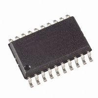
T5761-TGS Atmel, T5761-TGS Datasheet - Page 6

T5761-TGS
Manufacturer Part Number
T5761-TGS
Description
IC RCVR902-928MHZ ASK/FSK 20SOIC
Manufacturer
Atmel
Datasheet
1.T5761-TGQ.pdf
(35 pages)
Specifications of T5761-TGS
Frequency
915MHz
Sensitivity
-110dBm
Data Rate - Maximum
10 kBaud
Modulation Or Protocol
ASK, FSK
Applications
General Purpose Data Transmission Systems
Current - Receiving
7.8mA
Data Interface
PCB, Surface Mount
Antenna Connector
PCB, Surface Mount
Voltage - Supply
4.5 V ~ 5.5 V
Operating Temperature
-40°C ~ 105°C
Package / Case
20-SOIC (0.300", 7.50mm Width)
Lead Free Status / RoHS Status
Contains lead / RoHS non-compliant
Features
-
Memory Size
-
FSK/ASK Demodulator
and Data Filter
6
T5760/T5761
Since different RF input networks may exhibit slightly different values for the LNA gain,
the sensitivity values given in the electrical characteristics refer to a specific input
matching. This matching is illustrated in Figure 33 and exhibits the best possible sensi-
tivity and at the same time power matching at RF_IN.
R
switched from full sensitivity to reduced sensitivity or vice versa at any time. In polling
mode, the receiver will not wake up if the RF input signal does not exceed the selected
sensitivity. If the receiver is already active, the data stream at Pin DATA will disappear
when the input signal is lower than defined by the reduced sensitivity. Instead of the
data stream, the pattern according to Figure 5 is issued at Pin DATA to indicate that the
receiver is still active (see Figure 32).
Figure 5. Steady L State Limited DATA Output Pattern
The signal coming from the RSSI amplifier is converted into the raw data signal by the
ASK/FSK demodulator. The operating mode of the demodulator is set via the bit
ASK/_FSK in the OPMODE register. Logic ‘L’ sets the demodulator to FSK, applying ‘H’
to ASK mode.
In ASK mode an automatic threshold control circuit (ATC) is employed to set the detec-
tion reference voltage to a value where a good signal to noise ratio is achieved. This
circuit also implies the effective suppression of any kind of in-band noise signals or com-
peting transmitters. If the S/N (ratio to suppress in-band noise signals) exceeds about
10 dB the data signal can be detected properly, but better values are found for many
modulation schemes of the competing transmitter.
The FSK demodulator is intended to be used for an FSK deviation of 10 kHz £ Df £
100 kHz. In FSK mode the data signal can be detected if the S/N (ratio to suppress in-
band noise signals) exceeds about 2 dB. This value is valid for all modulation schemes
of a disturber signal.
The output signal of the demodulator is filtered by the data filter before it is fed into the
digital signal processing circuit. The data filter improves the S/N ratio as its passband
can be adopted to the characteristics of the data signal. The data filter consists of a 1
order high pass and a 2
The highpass filter cut-off frequency is defined by an external capacitor connected to Pin
CDEM. The cut-off frequency of the highpass filter is defined by the following formula:
In self-polling mode, the data filter must settle very rapidly to achieve a low current con-
sumption. Therefore, CDEM cannot be increased to very high values if self-polling is
used. On the other hand CDEM must be large enough to meet the data filter require-
ments according to the data signal. Recommended values for CDEM are given in the
electrical characteristics.
The cut-off frequency of the lowpass filter is defined by the selected baud-rate range
(BR_Range). The BR_Range is defined in the OPMODE register (refer to chapter
‘Configuration of the Receiver’). The BR_Range must be set in accordance to the used
baud-rate.
fcu_DF
Sens
can be connected to V
=
---------------------------------------------------------- -
2 p
´
´
30 kW
DATA
1
nd-
´
order lowpass filter.
t
CDEM
DATA_min
S
or GND via a microcontroller. The receiver can be
t DATA_L_max
4561B–RKE–10/02
st-


