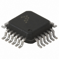
MC33591FTAR2 Freescale Semiconductor, MC33591FTAR2 Datasheet - Page 16

MC33591FTAR2
Manufacturer Part Number
MC33591FTAR2
Description
IC RF RECEIVER 315,434MHZ 24LQFP
Manufacturer
Freescale Semiconductor
Datasheet
1.MC33591MOD315.pdf
(28 pages)
Specifications of MC33591FTAR2
Frequency
315MHz, 434MHz
Sensitivity
-105dBm
Data Rate - Maximum
11 kBaud
Modulation Or Protocol
FSK, OOK
Applications
General Data Transfer
Current - Receiving
5.7mA
Data Interface
PCB, Surface Mount
Antenna Connector
PCB, Surface Mount
Voltage - Supply
1.9 V ~ 3.6 V
Operating Temperature
-40°C ~ 85°C
Package / Case
24-LQFP
Lead Free Status / RoHS Status
Contains lead / RoHS non-compliant
Features
-
Memory Size
-
Other names
MC33591FTAR2TR
STROBE OSCILLATOR
Programming SOE=0 sets ROMEO2 to state 6. The circuit is in Sleep mode.
A high level applied on STROBE sets the circuit into state 7. If an ID or its complement is detected, the state
machine advances to state 8. If not, it will stay in state 7 as long as STROBE is high.
After ID or its complement detection, ID byte is sent to the microcontroller on MOSI line at 310kBd. This warns
the microcontroller that data are received which means that an high level has to be maintained on STROBE. At
any time a low level applied on STROBE sets the circuit into state 6.
If Header or its complement is detected, the state machine advances to state 10. If not, it will stay in state 9 as
long as STROBE is high.
If Header has been received, data and clock signals are output on the SPI port. If the complement of Header has
been received, output data are complemented too. At any time a low level applied on STROBE sets the circuit
into state 6, after the current byte is fully transmitted.
If data are received after a End of Message they are output on the MOSI pin without clock recovery.
At any time, a low level applied on RESETB for more than one Ts forces the state machine to state 1. When the
transition condition from one state to the next one is fulfilled, the transition time is one Ts except reaching state 6.
The transition time for reaching state 6 is 2
low when in state 10).
STROBE OSCILLATOR
resistance R2 (refer to figure 17 and table 11). When a threshold is reached or exceeded C5 is discharged and
the cycle restarts. The period is: T
V
the STROBE pin is set to V
current which must be supplied.
16
CC
State 7:
State 8:
State 9:
State 10:
State 11:
For all states:
The Strobe Oscillator is a relaxation oscillator in which an external capacitor C5 is charged by an external
The circuit may be forced into states 0b, 3, 7 etc. (see State Machine Diagrams) by setting the STROBE pin to
. As V
CC
is above the oscillator threshold voltage referred to in the previous paragraph, the condition in which
CC
is internally detected and the oscillator pull-down circuitry disabled to limit the
Freescale Semiconductor, Inc.
Strobe
For More Information On This Product,
=0.12
MC33591 Technical Data
´
Go to: www.freescale.com
Ts (+ time needed to shift out a full byte if STROBE pin is forced to
´
R2
´
C5.
MOTOROLA


