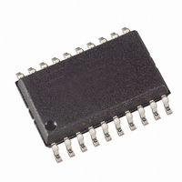
ATA3742P3-TGQY Atmel, ATA3742P3-TGQY Datasheet - Page 7

ATA3742P3-TGQY
Manufacturer Part Number
ATA3742P3-TGQY
Description
IC UHF ASK/FSK RECEIVER 20SOIC
Manufacturer
Atmel
Datasheet
1.ATA3742P3-TGQY.pdf
(34 pages)
Specifications of ATA3742P3-TGQY
Frequency
310MHz ~ 440MHz
Sensitivity
-108dBm
Data Rate - Maximum
10 kBaud
Modulation Or Protocol
ASK, FSK
Applications
RKE, TPM, Security Systems
Current - Receiving
7mA
Data Interface
PCB, Surface Mount
Antenna Connector
PCB, Surface Mount
Voltage - Supply
4.5 V ~ 5.5 V
Operating Temperature
-40°C ~ 105°C
Package / Case
20-SOIC (0.300", 7.50mm Width)
Operating Frequency (max)
450000kHz
Operating Temperature (min)
-40C
Operating Temperature (max)
105C
Operating Temperature Classification
Industrial
Operating Supply Voltage (min)
4.5V
Operating Supply Voltage (typ)
5V
Operating Supply Voltage (max)
5.5V
Lead Free Status / RoHS Status
Lead free / RoHS Compliant
Features
-
Memory Size
-
Lead Free Status / Rohs Status
Compliant
Other names
ATA3742P3-TGQYTR
4. Analog Signal Processing
4.1
4.2
4.3
4900B–RKE–11/07
IF Amplifier
RSSI Amplifier
Pin RSSI
The signals coming from the RF front end are filtered by the fully integrated 4th-order IF filter.
T h e I F c e n t e r f r e q u e n c y i s f
f
the center frequency.
The receiver ATA3742-M3 employs an IF bandwidth of B
with the U2741B in FSK and ASK mode.
The subsequent RSSI amplifier enhances the output signal of the IF amplifier before it is fed into
the demodulator. The dynamic range of this amplifier is R
operated within its linear range, the best signal-to-noise ratio (SNR) is maintained in ASK mode.
If the dynamic range is exceeded by the transmitter signal, the SNR is defined by the ratio of the
maximum RSSI output voltage and the RSSI output voltage due to a disturber. The dynamic
range of the RSSI amplifier is exceeded if the RF input signal is about 60 dB higher compared to
the RF input signal at full sensitivity.
In FSK mode, the SNR is not affected by the dynamic range of the RSSI amplifier.
The output voltage of the RSSI amplifier is internally compared to a threshold voltage V
V
pin SENS and GND or V
this means, it is possible to operate the receiver at a lower sensitivity.
The output voltage of the RSSI amplifier (V
signal, the signal strength of different transmitters can be distinguished.
The usable input-power range P
V
lute level of each transmitter, but the level differences can be used to distinguish several
transmitters. As illustrated in
the temperature range.
sation of V
RF
Th_red
RSSI
= 433.92 MHz is used. For other RF input frequencies, see
is typically
is determined by the value of the external resistor R
RSSI
.
–
2.2 mV/K. Due to TC and gain tolerance, it is not possible to find out the abso-
Figure 4-1
S
. The output of the comparator is fed into the digital control logic. By
Figure 4-2 on page
Ref
I F
illustrates an application that realizes a temperature compen-
is
= 1 M H z f o r a p p l i c a t i o n s w h e r e f
–
100 dBm to
RSSI
) is available at pin RSSI. Using the RSSI output
8, the RSSI output voltage is not constant over
–
55 dBm. The temperature coefficient TC of
IF
= 600 kHz and can be used together
RSSI
Sense
Table 3-1 on page 5
= 60 dB. If the RSSI amplifier is
. R
Sense
is connected between
R F
ATA3742
= 3 1 5 M H z o r
to determine
Th_red
7
.


