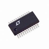
LT5500EGN Linear Technology, LT5500EGN Datasheet - Page 3

LT5500EGN
Manufacturer Part Number
LT5500EGN
Description
IC RECEIVER FRONT END 24-SSOP
Manufacturer
Linear Technology
Datasheet
1.LT5500EGN.pdf
(12 pages)
Specifications of LT5500EGN
Frequency
1.8GHz ~ 2.7GHz
Applications
HS Wireless LAN, Wireless Local Loop
Current - Receiving
23mA
Data Interface
PCB, Surface Mount
Antenna Connector
PCB, Surface Mount
Voltage - Supply
1.8 V ~ 5.25 V
Operating Temperature
-40°C ~ 85°C
Package / Case
24-SSOP
Pin Count
24
Screening Level
Industrial
Lead Free Status / RoHS Status
Contains lead / RoHS non-compliant
Features
-
Sensitivity
-
Memory Size
-
Data Rate - Maximum
-
Modulation Or Protocol
-
Lead Free Status / Rohs Status
Not Compliant
Available stocks
Company
Part Number
Manufacturer
Quantity
Price
Company:
Part Number:
LT5500EGN
Manufacturer:
LT
Quantity:
5 549
Part Number:
LT5500EGN
Manufacturer:
LINEAR/凌特
Quantity:
20 000
Part Number:
LT5500EGN#PBF
Manufacturer:
LINEAR/凌特
Quantity:
20 000
Part Number:
LT5500EGN#TRPBF
Manufacturer:
LINEAR/凌特
Quantity:
20 000
ELECTRICAL CHARACTERISTICS
LNA: f
SYMBOL
(Test circuit shown in Figure 3 for 2.5GHz application) V
P
SYMBOL
LNA High Gain: EN = 1.35V, GS = 1.35V
LNA Low Gain: EN = 1.35V, GS = 0.3V
Mixer: EN = 1.35V, GS = 1.35V
V
SYMBOL
Power Supply
V
I
I
I
I
I
Note 1: Absolute Maximum Ratings are those values beyond which the life of
the device may be impaired.
Note 2: LO Absolute Maximum Ratings apply for each LO pin separately.
Note 3: Component values listed in Figure 3 for 1.8GHz evaluation board were
used to guarantee 1.8GHz performance.
CC
CC
CC
EN
GS
CC
LO
CC
HG
LG
Off
= –10dBm, T
= 3V DC, T
LNA_IN
PARAMETER
LO Frequency Range (Note 4)
IF Frequency Range (Note 3)
LO-IF Isolation
LO-RF Isolation
RF-LO Isolation
PARAMETER
Forward Gain
Reverse Gain (Isolation)
Noise Figure
Input Return Loss
Output Return Loss
Input 1dB Compression
Input 3rd Order Intercept
Forward Gain
Reverse Gain (Isolation)
Noise Figure
Input 1dB Compression
Input 3rd Order Intercept
Conversion Gain
SSB Noise Figure
Input P1dB
Input 3rd Order Intercept
LO-IF Isolation
LO-RF Isolation
RF-LO Isolation
PARAMETER
Supply Voltage
Rx High Gain Mode
Rx Low Gain Mode
Shutdown Current
Enable Current
Gain Select Current
= 1.8GHz, Mixer: f
A
= 25°C (Note 4)
A
= 25°C, unless otherwise noted.
MIX_IN
= 1.8GHz, f
LO
= 1.52GHz, P
CONDITIONS
Matching Required
Matching Required
CONDITIONS
Terminated 50Ω Source
No External Matching
With External Matching
Two Tone Test, ∆f = 2MHz
Two Tone Test, ∆f = 2MHz
Terminated 50Ω Source
Two Tone Test, ∆f = 2MHz
CONDITIONS
EN = 1.35V, GS = 1.35V
EN = 1.35V, GS = 0.3V
EN = 0.3V, GS = 0.3V
EN = 1.35V (Note 5)
GS = 1.35V (Note 6)
CC
(Test circuit shown in Figure 3 for 1.8GHz application) V
= 3V DC, LNA: f
LO
= –10dBm, T
Note 4: Specifications over the –40°C to 85°C operating temperature range
are assured by design, characterization and correlation with statistical process
controls.
Note 5: When EN ≤ 0.3V, enable current is <10µA.
Note 6: When GS ≤ 0.3V, gain select current is <10µA.
LNA_IN
A
= 2.5GHz, Mixer: f
= 25°C, unless otherwise noted. (Notes 3, 4)
MIX_IN
MIN
MIN
MIN
= 2.5GHz, f
0.01 to 3.15
1.8 to 5.25
10 to 450
–3.5
– 2.5
TYP
13.5
TYP
–35
–15
–14
–39
–11
TYP
9.5
–1
36
36
40
12
15
19
33
37
32
23
18
21
21
4
8
5
2
CC
LO
= 3V DC,
MAX
MAX
MAX
= 2.22GHz,
33
31
25
LT5500
UNITS
UNITS
UNITS
3
dBm
dBm
dBm
dBm
dBm
dBm
MHz
5500f
GHz
mA
mA
dB
dB
dB
dB
dB
dB
dB
dB
dB
dB
dB
dB
dB
dB
dB
dB
µA
µA
µA
V


