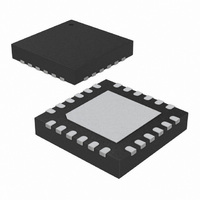
ATA5746-PXQW Atmel, ATA5746-PXQW Datasheet - Page 20

ATA5746-PXQW
Manufacturer Part Number
ATA5746-PXQW
Description
IC RCVR ASK/FSK UHF 24-QFN
Manufacturer
Atmel
Datasheet
1.ATA5745-EK.pdf
(44 pages)
Specifications of ATA5746-PXQW
Frequency
315MHz
Sensitivity
-114dBm
Data Rate - Maximum
10 kbps
Modulation Or Protocol
ASK, FSK
Applications
Alarm and Security Systems, RKE, TPMS
Current - Receiving
6.7mA
Data Interface
PCB, Surface Mount
Antenna Connector
PCB, Surface Mount
Voltage - Supply
2.7 V ~ 3.3 V, 4.5 V ~ 5.5 V
Operating Temperature
-40°C ~ 105°C
Package / Case
24-VQFN Exposed Pad, 24-HVQFN, 24-SQFN, 24-DHVQFN
Lead Free Status / RoHS Status
Lead free / RoHS Compliant
Features
-
Memory Size
-
Available stocks
Company
Part Number
Manufacturer
Quantity
Price
Company:
Part Number:
ATA5746-PXQW
Manufacturer:
ATMEL
Quantity:
3
5. Power Supply
5.1
5.2
20
OFF Mode
Standby Mode
ATA5745/ATA5746 [Preliminary]
Figure 5-1.
The supply voltage range of the ATA5745/ATA5746 is 2.7V to 3.3V or 4.5V to 5.5V.
Pin VS3V_AVCC is the supply voltage input for the range 2.7V to 3.3V, and is used in battery
applications using a single lithium 3V cell. Pin VS5V is the voltage input for the range 4.5V to
5.5V (car applications) in this case the voltage regulator V_REG regulates VS3V_AVCC to typi-
cally 3.0V. If the voltage regulator is active, a blocking capacitor of 2.2 µF has to be connected to
VS3V_AVCC (see
DVCC is the internal operating voltage of the digital control logic and is fed via the switch
SW_DVCC by VS3V_AVCC. DVCC must be blocked on pin DVCC with 68 nF (see
on page 27
Pin RX is the input to activate the RX signal processing and set the receiver to Active mode.
A low level on pin RX and ENABLE will set the receiver to OFF mode (low power mode). In this
mode, the crystal oscillator is shut down and no clock is available on pin CLK_OUT. The
receiver is not sensitive to a transmitter signal in this mode.
Table 5-1.
The receiver activates the Standby mode if pin ENABLE is set to “1”.
In Standby mode, the XTO is running and the clock on pin CLK_OUT is available after the
start-up time of the XTO ha s elapsed (dependent on pin CLK_OUT_CTRL0 an d
CLK_OUT_CTRL1). During Standby mode, the receiver is not sensitive to a transmitter signal.
In Standby mode, the RX signal path is disabled and the power consumption I
50 µA (CLK_OUT output off, VS3V_AVCC = VS5V = 3V). The exact value of this current is
strongly dependent on the application and the exact operation mode, therefore check the sec-
tion
VS3V_AVCC
“Electrical Characteristics: General” on page 29
VS5V
RX
RX
0
and
Power Supply
Standby Mode
Figure 10-1 on page
Figure 10-1 on page
ENABLE
IN
28).
0
28).
3.0V typ.
V_REG
EN
OUT
for the appropriate application case.
SW_DVCC
OFF mode
Function
Standby
4596B–RKE–06/07
Figure 9-1
is typically
DVCC


