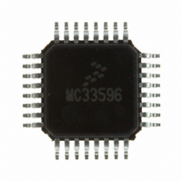
MC33596FJE Freescale Semiconductor, MC33596FJE Datasheet - Page 33

MC33596FJE
Manufacturer Part Number
MC33596FJE
Description
IC RECEIVER UHF PLL TUNED 32LQFP
Manufacturer
Freescale Semiconductor
Type
Receiverr
Datasheet
1.MC33596FCAE.pdf
(70 pages)
Specifications of MC33596FJE
Frequency
304, 315, 426, 434, 868 & 915MHz
Sensitivity
-104dBm
Data Rate - Maximum
22.4 kBaud
Modulation Or Protocol
FSK, OOK
Applications
General Data Transfer
Current - Receiving
10.3mA
Data Interface
PCB, Surface Mount
Antenna Connector
PCB, Surface Mount
Voltage - Supply
2.7 V ~ 3.6 V, 4.5 V ~ 5.5 V
Operating Temperature
-40°C ~ 85°C
Package / Case
32-LQFP
Operating Frequency
915 MHz
Operating Supply Voltage
3.3 V or 5 V
Maximum Operating Temperature
+ 85 C
Minimum Operating Temperature
- 40 C
Mounting Style
SMD/SMT
Operating Temperature (min)
-40C
Operating Temperature (max)
85C
Operating Temperature Classification
Industrial
Modulation Type
FSK/OOK
Package Type
LQFP
Operating Supply Voltage (min)
2.7V
Lead Free Status / RoHS Status
Lead free / RoHS Compliant
Features
-
Memory Size
-
Lead Free Status / Rohs Status
Lead free / RoHS Compliant
Available stocks
Company
Part Number
Manufacturer
Quantity
Price
Part Number:
MC33596FJE
Manufacturer:
FREESCALE
Quantity:
20 000
Part Number:
MC33596FJER2
Manufacturer:
FREESCALE
Quantity:
20 000
15.1.3.1 BANKA = X, BANKB = 0
If strobe pin is 1, configuration is defined by Bank A, BANKS = 1.
If strobe pin is 0, MC33596 configuration is OFF.
If a message is received during State A, current state remains State A up to end of message.
15.1.3.2 BANKA = 0, BANKB = 1
If strobe pin is 1, configuration is defined by Bank B, BANKS = 0.
If strobe pin is 0, MC33596 configuration is OFF.
If a message is received during State B, current state remains State B up to end of message.
15.1.3.3 BANKA = 1, BANK B = 1
BANKS toggles at the end of each state A or state B.
If strobe is forced to 1, configuration is frozen according to BANKS value.
If a read or write access is done using SPI, the next sequence will begin with state A in whatever was the
active state before SPI access by MCU.
For all available sequences:
Freescale Semiconductor
Strobe
Banks
Banks Bit
State A
State A
A
•
•
•
•
•
•
State B
1
Z
State A and State B are defined by Bank A and Bank B.
State A duration, TonA is defined by Bank A RON[3–0].
State B duration, TonB is defined by Bank B RON[3–0].
OFF duration, TonB is defined by Bank A ROFF[2–0].
If strobe pin is 1, the state is ON and defined by BANKS at that time. It remains this state up to
the release of strobe and end of message if a message is being received.
If a message is being received during State A or B, current state remains State A or B up to end of
message.
B
State B
OFF
OFF
OFF
A
B
OFF
State A
MC33596 Data Sheet, Rev. 4
OFF
State B
StateA
A
OFF
StateB
B
OFF
OFF
State A
Configuration Switching
State B
A
OFF
B
33


