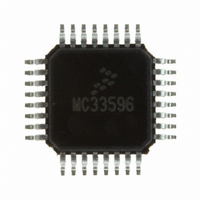
MC33596FJE Freescale Semiconductor, MC33596FJE Datasheet - Page 43

MC33596FJE
Manufacturer Part Number
MC33596FJE
Description
IC RECEIVER UHF PLL TUNED 32LQFP
Manufacturer
Freescale Semiconductor
Type
Receiverr
Datasheet
1.MC33596FCAE.pdf
(70 pages)
Specifications of MC33596FJE
Frequency
304, 315, 426, 434, 868 & 915MHz
Sensitivity
-104dBm
Data Rate - Maximum
22.4 kBaud
Modulation Or Protocol
FSK, OOK
Applications
General Data Transfer
Current - Receiving
10.3mA
Data Interface
PCB, Surface Mount
Antenna Connector
PCB, Surface Mount
Voltage - Supply
2.7 V ~ 3.6 V, 4.5 V ~ 5.5 V
Operating Temperature
-40°C ~ 85°C
Package / Case
32-LQFP
Operating Frequency
915 MHz
Operating Supply Voltage
3.3 V or 5 V
Maximum Operating Temperature
+ 85 C
Minimum Operating Temperature
- 40 C
Mounting Style
SMD/SMT
Operating Temperature (min)
-40C
Operating Temperature (max)
85C
Operating Temperature Classification
Industrial
Modulation Type
FSK/OOK
Package Type
LQFP
Operating Supply Voltage (min)
2.7V
Lead Free Status / RoHS Status
Lead free / RoHS Compliant
Features
-
Memory Size
-
Lead Free Status / Rohs Status
Lead free / RoHS Compliant
Available stocks
Company
Part Number
Manufacturer
Quantity
Price
Part Number:
MC33596FJE
Manufacturer:
FREESCALE
Quantity:
20 000
Part Number:
MC33596FJER2
Manufacturer:
FREESCALE
Quantity:
20 000
00h CONFIG1-A
Bit Name
Reset
Value
0 =
1 =
01h CONFIG2-A
Bit Name
Reset
Value
0 =
1 =
02h CONFIG3-A
Bit Name
Reset
Value
0 =
1 =
03h COMMAND-A
Bit Name
Reset
Value
0 =
1 =
04h F1-A
Bit Name
Reset
Value
05h F2-A
Bit Name
Reset
Value
Bit 7
LOF1
1
R/W
304–434
315–916
Bit 7
DSREF
0
R/W
Fixed
Adaptive
Bit 7
AFF1
0
R/W
0.5–1
kHz
2–4 kHz
Bit 7
AFFC
0
R/W
AFFx
OFF
AFFx ON –20 dB
Bit 7
—
0
R/W
Bit 7
F7
0
R/W
91 h
Bit 6
LOF0
0
R/W
304–315
434–916
10 h
Bit 6
FRM
0
R/W
Friendly
Direct
30 h
Bit 6
AFF0
0
R/W
0.5–2
kHz
1–4 kHz
9 h
Bit 6
IFLA
0
R/W
No
48 h
Bit 6
—
1
R/W
0 h
Bit 6
F6
0
R/W
Bit 5
CF1
0
R/W
315–434
868
Bit 5
MODU
0
R/W
OOK
FSK
Bit 5
OLS
1
R
RAS
Unlocked Low V
Bit 5
—
0
R/W
RX
TX
Bit 5
—
0
R/W
Bit 5
F5
0
R/W
Bank A Registers
Bit 4
CF0
1
R/W
314
434–868
Bit 4
DR1
1
R/W
2.4–4.8
9.6–19.2
Bit 4
LVDS
1
RR
RAS
Bit 4
RSSIE
0
R/W
No
Yes
Bit 4
—
0
R/W
Bit 4
F4
0
R/W
Bit 3
RESET
0
R/W
No
Yes
Bit 3
DR0
0
R/W
2.4–9.6
4.8–19.2
Bit 3
ILA1
0
R/W
0–8 dB
14–24 dB 8–24 dB
Bit 3
EDD
1
R/W
Slow dec. No
Fast dec. Yes
Bit 3
F11
1
R/W
Bit 3
F3
0
R/W
Bit 2
SL
0
R/W
T/R
R/T
Bit 2
TRXE
0
R/W
Standby
Enable
Bit 2
ILA0
0
R/W
0–14 dB
Bit 2
RAGC
0
R/W
Bit 2
F10
0
R/W
Bit 2
F1
0
R/W
No
—
Bit 1
LVDE
0
R/W
Yes
Bit 1
DME
0
R/W
No
Yes
Bit 1
0
R/W
0–8 dB
14–24 dB 8–24 dB
Bit 1
FAGC
0
R/W
No
Yes
Bit 1
F9
0
R/W
Bit 1
F1
0
R/W
Figure 33. Bank Registers
Bit 0
CLKE
1
R/W
No
Yes
Bit 0
SOE
0
R/W
No
Yes
Bit 0
—
0
R/W
0–14 dB
Bit 0
BANKS
1
R
B Bank
A Bank
Bit 0
F8
0
R/W
Bit 0
F0
0
R/W
0Dh CONFIG1-B
Bit Name
Reset
Value
0 =
1 =
0Eh CONFIG2-B
Bit Name
Reset
Value
0 =
1 =
0Fh CONFIG3-B
Bit Name
Reset
Value
0 =
1 =
10h COMMAND-B
Bit Name
Reset
Value
0 =
1 =
11h F1-B
Bit Name
Reset
Value
12h F2-B
Bit Name
Reset
Value
Bit 7
LOF1
1
R/W
304–434
315–916
Bit 7
DSREF
0
R/W
Fixed
Adaptive
Bit 7
AFF1
0
R/W
0.5–1
kHz
2–4 kHz
Bit 7
AFFC
0
R/W
AFFx
OFF
AFFx ON –20 dB
Bit 7
—
0
R/W
Bit 7
F7
0
R/W
91 h
Bit 6
LOF0
0
R/W
304–315
434–916
10 h
Bit 6
FRM
0
R/W
Friendly
Direct
30 h
Bit 6
AFF0
0
R/W
0.5–2
kHz
1–4 kHz
9 h
Bit 6
IFLA
0
R/W
No
4800 h
Bit 6
—
1
R/W
0 h
Bit 6
F6
0
R/W
Bit 5
CF1
0
R/W
315–434
868
Bit 5
MODU
0
R/W
OOK
FSK
Bit 5
OLS
1
R[A]
RAS
Unlocked Low V
Bit 5
—
0
R/W
RX
TX
Bit 5
—
0
R/W
Bit 5
F5
0
R/W
Bank B Registers
Bit 4
CF0
1
R/W
314
434–868
Bit 4
DR1
1
R/W
2.4–4.8
9.6–19.2
Bit 4
LVDS
1
RR[A]
RAS
Bit 4
RSSIE
0
R/W
No
Yes
Bit 4
—
0
R/W
Bit 4
F4
0
R/W
Bit 3
—
—
—
Bit 3
DR0
Bit 3
ILA1
0–8 dB
F11
Bit 3
F3
0
R
0
R/W
2.4–9.6
4.8–19.2
0
R/W
14–24 dB 8–24 dB
Bit 3
EDD
1
R/W
Slow dec. No
Fast dec. Yes
Bit 3
1
R/W
0
R/W
Bit 2
SL
0
R/W
T/R
R/T
Bit 2
TRXE
0
R/W
Standby
Enable
Bit 2
ILA0
0
R/W
0–14 dB
Bit 2
RAGC
0
R/W
Bit 2
F10
0
R/W
Bit 2
F1
0
R/W
Bit 1
LVDE
0
R/W
No
Yes
Bit 1
DME
0
R/W
No
Yes
Bit 1
—
0
R/W
0–8 dB
14–24 dB 8–24 dB
Bit 1
FAGC
0
R/W
No
Yes
Bit 1
F9
0
R/W
Bit 1
F1
0
R/W
Bit 0
CLKE
1
No
Yes
Bit 0
SOE
0
No
Bit 0
—
0
0–14 dB
Bit 0
1
B Bank
Bit 0
F8
0
Bit 0
F0
0
R/W
R[A]
Yes
R/W
BANKS
R[A]
A Bank
R/W
R/W


