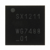
SX1211I084TRT Semtech, SX1211I084TRT Datasheet - Page 72

SX1211I084TRT
Manufacturer Part Number
SX1211I084TRT
Description
IC SNGL-CHIP TXRX 32-TQFN
Manufacturer
Semtech
Specifications of SX1211I084TRT
Frequency
860 ~ 960MHz
Data Rate - Maximum
200kbps
Modulation Or Protocol
FSK, OOK
Applications
AMR, ISM, Security and Access
Power - Output
12.5dBm
Sensitivity
-113dBm
Voltage - Supply
2.1 V ~ 3.6 V
Current - Receiving
3mA
Current - Transmitting
25mA
Data Interface
PCB, Surface Mount
Antenna Connector
PCB, Surface Mount
Operating Temperature
-40°C ~ 85°C
Package / Case
32-TQFN
Operating Temperature (min)
-40C
Operating Temperature (max)
85C
Operating Temperature Classification
Industrial
Modulation Type
FSK/OOK
Package Type
TQFN EP
Operating Supply Voltage (min)
2.1V
Operating Supply Voltage (typ)
2.5/3.3V
Operating Supply Voltage (max)
3.6V
Lead Free Status / RoHS Status
Lead free / RoHS Compliant
Memory Size
-
Lead Free Status / Rohs Status
Compliant
Other names
SX1211I084TRT
Available stocks
Company
Part Number
Manufacturer
Quantity
Price
Company:
Part Number:
SX1211I084TRT
Manufacturer:
HITTITE
Quantity:
560
A power-on reset of the SX1211 is triggered at power up. Additionally, a manual reset can be issued by controlling
pin 13.
If the application requires the disconnection of VDD from the SX1211, despite of the extremely low Sleep Mode
current, the user should wait for 10 ms from of the end of the POR cycle before commencing communications over
the SPI bus. Pin 13 (TEST8) should be left floating during the POR sequence.
Please note that any CLKOUT activity can also be used to detect that the chip is ready.
A manual reset of the SX1211 is possible even for applications in which VDD cannot be physically disconnected.
Pin 13 should be pulled high for a hundred microseconds, and then released. The user should then wait for 5 ms
before using the chip.
Please note that while pin 13 is driven high, an over current consumption of up to ten milliamps can be seen on
VDD.
Rev 7 – Sept 2
ADVANCED COMMUNICATIONS & SENSING
7.4. Reset of the Chip
7.4.1. POR
7.4.2. Manual Reset
nd
, 2008
VDD
Pin 13
(input)
VDD
Pin 13
(output)
Undefined
Figure 55: Manual Reset Timing Diagram
Figure 54: POR Timing Diagram
High-Z
Wait for
10 ms
> 100 us
Page 72 of 92
’’1’’
Chip is ready from
this point on
High-Z
Wait for
5 ms
Chip is ready from
this point on
www.semtech.com
SX1211


