DNT2400P RFM, DNT2400P Datasheet - Page 4
DNT2400P
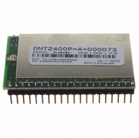
Manufacturer Part Number
DNT2400P
Description
TXRX MOD 2.4GHZ FHSS WITH I/O
Manufacturer
RFM
Datasheet
1.DNT2400DK.pdf
(7 pages)
Specifications of DNT2400P
Frequency
2.4GHz
Data Rate - Maximum
500kbps
Modulation Or Protocol
FSK/MSK
Power - Output
63mW
Sensitivity
-104dBm
Voltage - Supply
3.3 V ~ 5.5 V
Current - Receiving
105mA
Current - Transmitting
300mA
Data Interface
PCB, Through Hole
Antenna Connector
U.FL
Operating Temperature
-40°C ~ 85°C
Package / Case
Module
Product
RF Modules
Maximum Frequency
2.4 GHz
Output Power
1 mW, 10 mW, 63 mW
Supply Voltage (max)
5.5 V
Supply Current
105 mA
Maximum Operating Temperature
+ 85 C
Board Size
2 in x 1.26 in x 0.18 in
Lead Free Status / RoHS Status
Lead free / RoHS Compliant
Applications
-
Memory Size
-
Lead Free Status / Rohs Status
Lead free / RoHS Compliant
For Use With/related Products
DNT2400
Other names
583-1148
Available stocks
Company
Part Number
Manufacturer
Quantity
Price
Company:

Part Number:
DNT2400P
Manufacturer:
RFM
Quantity:
12 800


DNT2400 I/O Descriptions
www.RFM.com E-mail: info@rfm.com
©2009 by RF Monolithics, Inc.
Pin
10
11
12
13
14
15
16
17
18
19
20
21
22
23
24
25
26
27
28
29
1
2
3
4
5
6
7
8
9
SLEEP/DTR
ADC_REF
EX_SYNC
PKT_DET
DIAG_RX
DIAG_TX
GPIO0
GPIO1
GPIO2
GPIO3
PWM0
PWM1
GPIO4
GPIO5
Name
RSVD
RSVD
RSVD
RSVD
RSVD
ADC2
ADC1
ADC0
/CFG
/DCD
VCC
GND
GND
GND
ACT
I/O
I/O
I/O
I/O
I/O
I/O
I/O
O
O
O
O
O
O
-
-
-
-
-
-
-
-
I
I
I
I
I
I
I
I
I
Packet detect output. Signal switches logic high at the end of the start-of-packet symbol and switches logic
low at the end of the end-of-packet symbol on both received and transmitted packets. PKT_DET provides a
timing reference for external use in network timing evaluations, etc.
Reserved pin. Leave unconnected.
ADC supply and external full scale reference voltage input. Voltage range is 2.4 to 3.3 Vdc. Connect pad 34 to
this input to reference the ADC full scale reading to the module’s 3.3 V regulated supply.
Reserved pin. Leave unconnected.
Configurable digital I/O port 0. When configured as an input, an internal pull-up resistor can be selected and
interrupt from sleep can be invoked. When configured as an output, the power-on state is also configurable.
Configurable digital I/O port 1. Same configuration options as GPIO0.
Configurable digital I/O port 2. Same configuration options as GPIO0.
Configurable digital I/O port 3. Same configuration options as GPIO0.
8-bit pulse-width modulated output 0 with internal low-pass filter. Filter is first-order, with a159 Hz 3 dB
bandwidth.
8-bit pulse-width modulated output 1 with internal low-pass filter. Filter is first-order, with a 159 Hz 3 dB
bandwidth.
Active high module sleep input (active low DTR). When switched low after sleep, the module executes a
power on-reset. Usually connected to host DTR. Connect to ground if SLEEP/DTR function not used.
10-bit ADC input 0. Full scale reading is referenced to the ADC_REF input.
10-bit ADC input 1. Full scale reading is referenced to the ADC_REF input.
10-bit ADC input 2. Full scale reading is referenced to the ADC_REF input.
Rising-edge triggered input for synchronizing co-located base stations. Synchronization pulse interval must
equal hop dwell time ±10 µs. Pulse width must be in the range of 50 µs to 2 ms.
Diagnostic UART transmitter output.
Diagnostic UART receiver input.
Protocol selection input. Leave unconnected when using software commands to select transparent/protocol
mode (default is transparent mode). Logic low selects protocol mode, logic high selects transparent mode.
Power supply input, +3.3 to +5.5 Vdc.
Power supply and signal ground. Connect to the host circuit board ground.
Power supply and signal ground. Connect to the host circuit board ground.
Configurable digital I/O port 4. When configured as an input, an internal pull-up resistor can be selected.
When configured as an output, the power-on state is configurable.
Configurable digital I/O port 5. Same configuration options as GPIO4.
Logic ground.
Data activity output, logic high when data is being transmitted or received.
Default functionality is data carrier detect output, logic low on a remote when the module is locked to FHSS
hopping pattern and logic low on a base station when at least one remote is connected to it.
Reserved pin. Leave unconnected.
Reserved pin. Leave unconnected.
Reserved pin. Leave unconnected.
Description
DNT2400 - 08/12/09
Page 4 of 7
Related parts for DNT2400P
Image
Part Number
Description
Manufacturer
Datasheet
Request
R

Part Number:
Description:
ASH RX 115.2 KBPS 433.92 MHZ
Manufacturer:
RFM
Datasheet:

Part Number:
Description:
RFIC TRANCEIVER MULTI-CHANNEL FS
Manufacturer:
RFM
Datasheet:

Part Number:
Description:
ASH TX 115.2 KBPS 433.92 MHZ
Manufacturer:
RFM
Datasheet:
Part Number:
Description:
Filters 1602MHz BW=61MHz
Manufacturer:
RFM
Datasheet:

Part Number:
Description:
RESONATOR, SM3030-6
Manufacturer:
RFM
Datasheet:

Part Number:
Description:
RESONATOR, SM3030-6
Manufacturer:
RFM
Datasheet:

Part Number:
Description:
RESONATOR, SM3030-6
Manufacturer:
RFM
Datasheet:

Part Number:
Description:
RESONATOR, SM5035-4
Manufacturer:
RFM
Datasheet:
Part Number:
Description:
RESONATOR 418MHZ SM5035-4
Manufacturer:
RFM
Datasheet:
Part Number:
Description:
RESONATOR 315 MHZ SMD
Manufacturer:
RFM
Datasheet:

Part Number:
Description:
10-Terminal Ceramic Surface-Mount Case 7 x 5 mm Nominal Footprint
Manufacturer:
RFM [RF Monolithics, Inc]
Datasheet:
Part Number:
Description:
QUAD-BAND GSM850/GSM/DCS/PCS POWER AMP MODULE
Manufacturer:
RFM [RF Monolithics, Inc]
Datasheet:
Part Number:
Description:
402 to 405 MHz Medical Band Front-end Filter
Manufacturer:
RFM [RF Monolithics, Inc]
Datasheet:
Part Number:
Description:
674.03 MHz SAW Resonator
Manufacturer:
RFM [RF Monolithics, Inc]
Datasheet: