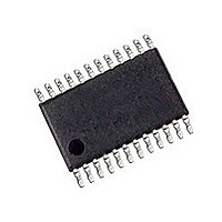
ADF7010BRU-REEL Analog Devices Inc, ADF7010BRU-REEL Datasheet - Page 16

ADF7010BRU-REEL
Manufacturer Part Number
ADF7010BRU-REEL
Description
IC ASK/FSK/GFSK BAND TX 24-TSSOP
Manufacturer
Analog Devices Inc
Datasheet
1.ADF7010BRUZ-REEL7.pdf
(20 pages)
Specifications of ADF7010BRU-REEL
Rohs Status
RoHS non-compliant
Frequency
902MHz ~ 928MHz
Applications
Data Transfer, RKE, Remote Control/Security Systems
Modulation Or Protocol
ASK, FSK, GFSK
Data Rate - Maximum
76.8 kbps
Power - Output
-16dBm ~ 12dBm
Current - Transmitting
40mA
Data Interface
PCB, Surface Mount
Antenna Connector
PCB, Surface Mount
Voltage - Supply
2.3 V ~ 3.6 V
Operating Temperature
-40°C ~ 85°C
Package / Case
24-TSSOP
Operating Temperature (min)
-40C
Operating Temperature (max)
85C
Operating Temperature Classification
Industrial
Product Depth (mm)
4.4mm
Operating Supply Voltage (min)
2.3V
Operating Supply Voltage (typ)
3.3V
Operating Supply Voltage (max)
3.6V
Features
-
Memory Size
-
Lead Free Status / Rohs Status
Not Compliant
ADF7010
Digital Lock Detect
Digital lock detect is active high. The lock detect circuit is
contained at the PFD. When the phase error on five consecutive
cycles is less than 15 ns, lock detect is set high. Lock detect
remains high until 25 ns phase error is detected at the PFD. Since
no external components are needed for digital lock detect, it is
more widely used than analog lock detect.
Analog Lock Detect
This N-channel open-drain lock detect should be operated with
an external pull-up resistor of 10 kW nominal. When lock has been
detected, this output will be high with narrow low going pulses.
VOLTAGE REGULATOR
The ADF7010 requires a stable voltage source for the VCO and
modulation blocks. The on-board regulator provides 2.2 V using
a band gap reference. A 2.2 mF capacitor from C
is used to improve stability of the regulator over a supply from 2.3 V
to 3.6 V. The regulator consumes less than 400 mA and can only
be powered down using the chip enable (CE) pin. Bringing
the chip enable pin low disables the regulator and also erases all
values held in the registers. The serial interface operates off the
regulator supply; therefore, to write to the part, the user must
have CE high. Regulator status can be monitored using the
Regulator Ready signal from MUXOUT.
LOOP FILTER
The loop filter integrates the current pulses from the charge
pump to form a voltage that tunes the output of the VCO to the
desired frequency. It also attenuates spurious levels generated
by the PLL. A typical loop filter design is shown in Figure 6.
ANALOG LOCK DETECT
DIGITAL LOCK DETECT
R COUNTER/2 OUTPUT
N COUNTER/2 OUTPUT
R COUNTER OUTPUT
N COUNTER OUTPUT
REGULATOR READY
REG
Figure 5. MUXOUT Stage
to ground
MUX
–16–
In FSK, the loop should be designed so that the loop bandwidth
(LBW) is approximately 5 times the data rate. Widening the LBW
excessively reduces the time spent jumping between frequencies
but may cause insufficient spurious attenuation.
For ASK systems, the wider the loop BW the better. The sudden
large transition between two power levels will result in VCO
pulling and can cause a wider output spectrum than is desired. By
widening the loop BW to >10 times the data rate, the amount
of the VCO pulling is reduced, since the loop will settle quickly
back to the correct frequency. The wider LBW may restrict the
output power and data rate of ASK based systems, compared
with FSK based systems.
Narrow loop bandwidths may result in the loop taking long
periods of time to attain lock. Careful design of the loop filter is
critical in obtaining accurate FSK/GFSK modulation.
For GFSK, it is recommended that an LBW of 2.0 to 2.5 times
the data rate be used to ensure sufficient samples are taken of the
input data while filtering system noise.
CONTROL
Figure 6. Typical Loop Filter Configuration––
Third Order Integrator
PUMP OUT
CHARGE
DGND
DV
DD
MUXOUT
VCO
REV. 0


