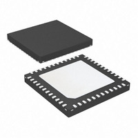
ATA5279P-PLQW Atmel, ATA5279P-PLQW Datasheet - Page 26

ATA5279P-PLQW
Manufacturer Part Number
ATA5279P-PLQW
Description
IC ANTENNA DVR SIX-FOLD 48QFN
Manufacturer
Atmel
Datasheet
1.ATA5279P-PLQW.pdf
(40 pages)
Specifications of ATA5279P-PLQW
Rf Type
PEG, TPMS
Frequency
125kHz
Features
RSSI Equipped
Package / Case
48-VQFN Exposed Pad, 48-HVQFN, 48-SQFN, 48-DHVQFN
Lead Free Status / RoHS Status
Lead free / RoHS Compliant
Available stocks
Company
Part Number
Manufacturer
Quantity
Price
Company:
Part Number:
ATA5279P-PLQW
Manufacturer:
ATMEL
Quantity:
3 500
Part Number:
ATA5279P-PLQW
Manufacturer:
ATMEL/爱特梅尔
Quantity:
20 000
3.10
3.11
26
Oscillator
Internal Supply
Atmel ATA5279
This block provides the clock signals internally needed for control logic, the LF driver stage,
and the boost converter. The oscillator requires an external clock source, which can either be
an active signal from a microcontroller for example, or a passive oscillation device like a crys-
tal or a ceramic resonator. As the LF carrier frequency is directly derived from this clock, the
(resonance) frequency of the clock source must be chosen to match the desired LF frequency.
Possible values range from 6.4MHz to 9.6MHz, where 8MHz is the typical value resulting in an
LF frequency of 125kHz.
Note that during start-up (i.e., as long as no stable oscillation can be detected), the driving cur-
rent for the crystal is increased to shorten the start-up delay. Furthermore, the IC is only
functional if the oscillator is working properly. That means, during start-up after a power-down
phase, no communication and no operation of the IC is possible until the oscillator reaches its
operation point.
If an external clock source such as a microcontroller is to be used, the logic-level clock signal
must be applied at the OSCI pin, and the OSCO pin must be left open. Note that the chip pro-
tection features, need a clock signal present at the OSCI pin; without this, the chip is not fully
protected. Therefore, if the chip is in any mode but in power-down (reset), a clock signal is
needed.
The oscillator block is, like the control logic and the SPI, supplied by the application-provided
logic supply voltage connected to the pin VIF.
The internal power supply stage provides all internally needed BIAS currents and reference
voltages. An integrated one-time-programming (OTP) structure is used to adjust internal set-
tings. This ensures parameter stability over the production process.
The internal supply block performs monitoring functions to reset or shut down the IC in case of
supply shortages or during power-up. A power-management minimizes current consumption
during power-down mode of the IC.
Another part of this block is the internal 5V voltage regulator. It is supplied by the VS pin, i.e.,
the battery supply connection. This voltage is used for all internal analog functions and driving
processes. It is active as long as the IC is not in power-down mode. To increase stability and
quality of this supply line, it is externally available (pin VCC) for connection to a ceramic
capacitor for filtering and buffering. Note that no loads must be connected to this pin.
As with the oscillator, this supply voltage must settle in its operation point prior to any opera-
tion. The control logic checks the status of this voltage and inhibits operation until it reaches
the required level. Furthermore, the driver supply voltage present on the VDSx pins is also
monitored. If the level falls below V
the Status Register) and driver-related commands cannot be processed. Once the voltage
level is valid again, the Op bit is set again, and operability is restored.
VDS,min
, the operability flag of the chip is cleared (bit Op in
9125L–RKE–03/11


