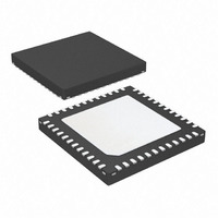
ATA5279P-PLQW Atmel, ATA5279P-PLQW Datasheet - Page 32

ATA5279P-PLQW
Manufacturer Part Number
ATA5279P-PLQW
Description
IC ANTENNA DVR SIX-FOLD 48QFN
Manufacturer
Atmel
Datasheet
1.ATA5279P-PLQW.pdf
(40 pages)
Specifications of ATA5279P-PLQW
Rf Type
PEG, TPMS
Frequency
125kHz
Features
RSSI Equipped
Package / Case
48-VQFN Exposed Pad, 48-HVQFN, 48-SQFN, 48-DHVQFN
Lead Free Status / RoHS Status
Lead free / RoHS Compliant
Available stocks
Company
Part Number
Manufacturer
Quantity
Price
Company:
Part Number:
ATA5279P-PLQW
Manufacturer:
ATMEL
Quantity:
3 500
Part Number:
ATA5279P-PLQW
Manufacturer:
ATMEL/爱特梅尔
Quantity:
20 000
8. Functional Parameters
All parameters valid for 7.0V VS 16.5V and –40°C T
32
*) Type means: A = 100% tested, B = 100% correlation tested, C = Characterized on samples, D = Design parameter
Notes:
1.10
1.11
1.12
No.
1.1
1.2
1.3
1.4
1.5
1.6
1.7
1.8
1.9
2.1
2.2
2.3
2.4
2.5
2.6
2.7
3.1
3.2
1
2
3
1. In this column, pin group names are given. Please refer to
2. Operation of coils with higher impedance than the given value is possible but functional limitations might occur (inability to
Parameters
Power Supply
VS-pin power-down
mode supply current
VS-pin idle mode
supply current
Internal VCC voltage
- idle
- load
VS voltage clamp
VCC power-on reset
threshold
VDS operation
threshold
Battery supply range for
normal operation
VDS power-down mode
supply current
VDS fault-shutdown
mode supply current
Battery supply range for
Jump start operation
VCC power-up time
Minimum VS voltage
level for VCC operation
Boost Converter
Overvoltage shut-down
level
Switch overcurrent
shutdown level
Switch on-state
resistance
Max duty cycle (t
Switch leakage current V
Switch fall time
Switch rise time
Oscillator
External clock source
frequency range
Driver output sink
resistance during
startup
Atmel ATA5279
more details.
reach to configured coil current). Coils with lower impedance should not be used as they might be detected as faulty.
on
/ T)
Test Conditions
V
V
7V VS 28V
I
I
VS = 28V
VS = 40V
VS = 16.5V
Idle mode
V
V
Idle mode
I
I
I
I
VCC
VCC
VL
VL
VL
OSCO
VS
VS
VDS
VDS
VL
= 200mA
= 200mA
= 500mA
= 38V
= 16.5V
= 0
= 5mA
= 28V
= 16.5V
14V
= 100µA
a
105°C unless otherwise noted.
CSP
CSP
BLS
BLS
BLS
BLS
BLS
BLS
Pin
DS
DS
DS
DS
1
1
4
1
4
1
1
4
1
Symbol
V
V
V
R
R
Section 2. “Pin Configuration” on page 2
V
I
V
V
I
I
I
I
D
I
PORVCC
I
VDS,FS
VS,C28
VS,C40
VDSmax
I
VDS,min
DSon,VL
VL,leak
VS,idle
VLmax
VDS,0
t
f
OSC,L1
V
V
VS,min
t
VSpd
t
VCC,0
VCC,1
VCC
OSC
Boost
VL,f
VL,r
VS
VS
Min.
0.85
200
4.8
1.5
4.1
5.1
2.9
6.4
0.9
50
40
50
50
7
0
7
6
Typ.
5.05
5.15
0.12
180
5.5
3.5
3.2
42
3
8
0.875
Max.
16.5
2.45
26.5
400
500
200
200
5.3
4.5
4.8
1.4
0.5
9.6
2.2
10
44
6
4
5
in this document for
MHz
Unit
mA
mA
mA
µA
µA
µA
nA
µs
ns
ns
k
V
V
V
V
V
V
V
A
-
9125L–RKE–03/11
Type*
D
D
D
D
D
A
A
A
A
A
A
A
A
A
A
A
A
A
A
A
A


