MCC95-12IO1B IXYS, MCC95-12IO1B Datasheet - Page 2
MCC95-12IO1B
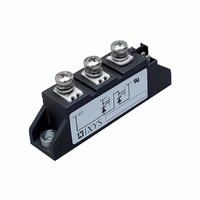
Manufacturer Part Number
MCC95-12IO1B
Description
THYRISTOR MODULE 1200V 2X116A
Manufacturer
IXYS
Type
SCR Moduler
Datasheet
1.MCC95-08I01B.pdf
(5 pages)
Specifications of MCC95-12IO1B
Structure
Series Connection - All SCRs
Number Of Scrs, Diodes
2 SCRs
Voltage - Off State
1200V
Current - Gate Trigger (igt) (max)
150mA
Current - On State (it (av)) (max)
116A
Current - On State (it (rms)) (max)
180A
Current - Non Rep. Surge 50, 60hz (itsm)
2250A, 2400A
Current - Hold (ih) (max)
200mA
Mounting Type
Chassis Mount
Package / Case
TO-240AA
Repetitive Peak Off-state Volt
1.2kV
Off-state Voltage
1.2kV
Average On-state Current
116A
Hold Current
200mA
Gate Trigger Current (max)
150mA
Gate Trigger Voltage (max)
2.5V
Peak Reverse Gate Voltage
10V
Package Type
TO-240AA
Peak Repeat Off Current
5mA
Peak Surge On-state Current (max)
2400A
On State Voltage(max)
1.5@300AV
Mounting
Screw
Pin Count
7
Operating Temp Range
-40C to 125C
Operating Temperature Classification
Automotive
Lead Free Status / RoHS Status
Lead free / RoHS Compliant
Available stocks
Company
Part Number
Manufacturer
Quantity
Price
Company:

Part Number:
MCC95-12IO1B
Manufacturer:
FUJI
Quantity:
300
Part Number:
MCC95-12IO1B
Quantity:
60


Optional accessories for modules
Coded gate/cathode twin plugs with wire length = 350 mm, gate = yellow, cathode = red
Type ZY 200L
Type ZY 200R
IXYS reserves the right to change limits, test conditions and dimensions.
© 2010 IXYS All rights reserved
Symbol
I
V
V
r
V
I
V
I
I
I
t
t
Q
I
R
R
d
d
a
RRM
GT
GD
L
H
RM
gd
q
t
GT
GD
S
A
T
T0
thJC
thJK
S
, V
, I
F
DRM
Conditions
V
I
For power-loss calculations only
V
V
V
t
I
V
V
I
V
dv/dt = 20 V/µs; -di/dt = 10 A/µs
I
I
per thyristor; DC current
per module
per thyristor; DC current
per module
Creeping distance on surface
Creepage distance in air
Maximum allowable acceleration
T
p
G
G
T
T
R
D
D
D
D
D
D
= 10 µs; V
/ I
= 150 A; V
/ I
= 0.45 A; di
= 0.45 A; di
/ V
= 6 V
= 6 V
=
= 6 V; R
= ½V
=
F
F
2
2
(L = Left for pin pair 4/5)
(R = Right for pin pair 6/7)
D
= 300 A
= 50 A; -di/dt = 6 A/µs
/
/
3
3
= V
V
V
DRM
DRM
DRM
RRM
GK
D
;
R
= 6 V
= ∞;
/ V
G
G
= 100 V; t
/dt = 0.45 A/µs
/dt = 0.45 A/µs
DRM
p
= 200 µs
other values
see Fig. 8/9
UL 758, style 1385,
CSA class 5851, guide 460-1-1
T
T
T
T
T
T
T
T
T
T
T
T
T
VJ
VJ
VJ
VJ
VJ
VJ
VJ
VJ
VJ
VJ
VJ
VJ
VJ
= T
= 25°C
= T
= 25°C
= -40°C
= 25°C
= -40°C
= T
= 25°C
= 25°C
= 25°C
= T
= T
VJM
VJM
VJM
VJM
VJM
Characteristic Values
185
typ.
max.
12.7
0.22
0.11
0.42
0.21
150
200
450
200
170
1.5
0.8
2.4
2.5
2.6
0.2
9.6
10
45
50
5
2
m/s
K/W
K/W
K/W
K/W
mm
mm
mW
mA
mA
mA
mA
mA
mA
µC
µs
µs
V
V
V
V
V
A
2
[V]
Fig. 1 Gate trigger characteristics
[µs]
Fig. 2 Gate trigger delay time
V
t
gd
G
100
100
0.1
0.1
10
10
1
0.01
1
0.01
P
P
GAV
GM
= 120 W
=
0.1
I
GD
60 W
t
t
8 W
p
p
0.1
= 30 µs
= 500 µs
I
I
G
G
1
[A]
[A]
I
I
I
GT
GT
GT
(T
(T
(T
MCC 95
MCD 95
1
VJ
VJ
VJ
10
T
limit
typ.
= -40°C)
= 0°C)
= 25°C)
VJ
= 25°C
20101116a
2 - 5
10
Related parts for MCC95-12IO1B
Image
Part Number
Description
Manufacturer
Datasheet
Request
R

Part Number:
Description:
DIODE MODULE RECTIFIER
Manufacturer:
IXYS
Datasheet:
Part Number:
Description:
MOD THYRISTOR DUAL 800V TO-240AA
Manufacturer:
IXYS
Datasheet:
Part Number:
Description:
MOD THYRISTOR DUAL 800V TO-240AA
Manufacturer:
IXYS
Datasheet:
Part Number:
Description:
THYRISTOR MODULE 1200V 2X116A
Manufacturer:
IXYS
Datasheet:
Part Number:
Description:
MOD THYRISTOR DUAL 1400V TO240AA
Manufacturer:
IXYS
Datasheet:
Part Number:
Description:
MOD THYRISTOR DUAL 1400V TO240AA
Manufacturer:
IXYS
Datasheet:
Part Number:
Description:
MOD THYRISTOR DUAL 1800V TO240AA
Manufacturer:
IXYS
Datasheet:
Part Number:
Description:
MOD THYRISTOR DUAL 1800V TO240AA
Manufacturer:
IXYS
Datasheet:
Part Number:
Description:
THYRISTOR MODULE 1600V TO-240AA
Manufacturer:
IXYS
Datasheet:
Part Number:
Description:
THYRISTOR MODULE 1600V 2X116A
Manufacturer:
IXYS
Datasheet:


Part Number:
Description:
Thyristor Modules Thyristor/Diode Modules
Manufacturer:
IXYS Corporation
Part Number:
Description:
1800V thyristor modules thyristor/diode module
Manufacturer:
IXYS Corporation