KAD5510P-21Q48 Intersil, KAD5510P-21Q48 Datasheet
KAD5510P-21Q48
Specifications of KAD5510P-21Q48
Available stocks


Related parts for KAD5510P-21Q48


KAD5510P-21Q48 Summary of contents
Page 1
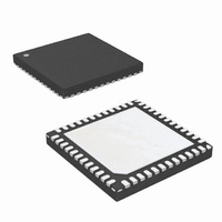
... Digital output data is presented in selectable LVDS or CMOS formats. The KAD5510P is available in a 48-contact QFN package with an exposed paddle. Operating from a 1.8V supply, performance is specified over the full industrial temperature range (-40°C to +85°C). ...
Page 2
... KAD5510P-25/21/17/12 Pin Configuration AVDD 1 DNC 2 3 DNC DNC 4 AVSS 5 6 VINN 7 VINP 8 AVSS AVDD 9 VCM 10 DNC 11 AVSS 12 2 KAD5510P RESOLUTION KAD5510P (48 LD QFN) TOP VIEW PAD CONNECT THERMAL PAD TO AVSS FIGURE 1. PIN CONFIGURATION PACKAGE SPEED (MSPS) Q48EP 250/210/170/125 X 500 250/210/170/125 X 250/210/170/125 X ...
Page 3
... PAD (Exposed Paddle) NOTE: LVCMOS Output Mode Functionality is shown in brackets ( Connection). 3 KAD5510P AVDD 1.8V Analog Supply DNC Do Not Connect AVSS Analog Ground Analog Input Negative, Positive VCM Common Mode Output Clock Input True, Complement Tri-Level Power Control (Nap, Sleep modes) Power On Reset (Active Low, see page 16) ...
Page 4
... Ordering Information PART NUMBER (Notes 1, 2) KAD5510P-25Q48 KAD5510P-25 Q48EP-I KAD5510P-21Q48 KAD5510P-21 Q48EP-I KAD5510P-17Q48 KAD5510P-17 Q48EP-I KAD5510P-12Q48 KAD5510P-12 Q48EP-I NOTES: 1. These Intersil Pb-free plastic packaged products employ special Pb-free material sets, molding compounds/die attach materials, and 100% matte tin plate plus anneal (e3 termination finish, which is RoHS compliant and compatible with both SnPb and Pb-free soldering operations). Intersil Pb- free products are MSL classified at Pb-free peak reflow temperatures that meet or exceed the Pb-free requirements of IPC/JEDEC J STD-020 ...
Page 5
... ADC Evaluation Platform . . . . . . . . . . . . . . . . . . . . . . . . . . . . . . . . . . . . . . . . . . . . . . . . . . . . . . . . . . . . . . . . . . . . . . . . . . . . . . . . 28 Layout Considerations PCB Layout Example . . . . . . . . . . . . . . . . . . . . . . . . . . . . . . . . . . . . . . . . . . . . . . . . . . . . . . . . . . . . . . . . . . . . . . . . . . . . . . . . . .28 Split Ground and Power Planes . . . . . . . . . . . . . . . . . . . . . . . . . . . . . . . . . . . . . . . . . . . . . . . . . . . . . . . . . . . . . . . . . . . . . . . . 28 Clock Input Considerations . . . . . . . . . . . . . . . . . . . . . . . . . . . . . . . . . . . . . . . . . . . . . . . . . . . . . . . . . . . . . . . . . . . . . . . . . . . . 28 Exposed Paddle . . . . . . . . . . . . . . . . . . . . . . . . . . . . . . . . . . . . . . . . . . . . . . . . . . . . . . . . . . . . . . . . . . . . . . . . . . . . . . . . . . . . . 28 Bypass and Filtering LVDS Outputs . . . . . . . . . . . . . . . . . . . . . . . . . . . . . . . . . . . . . . . . . . . . . . . . . . . . . . . . . . . . . . . . . . . . . . . . . . . . . . . . . . . . . . . 28 LVCMOS Outputs Unused Inputs . . . . . . . . . . . . . . . . . . . . . . . . . . . . . . . . . . . . . . . . . . . . . . . . . . . . . . . . . . . . . . . . . . . . . . . . . . . . . . . . . . . . . . . 28 General PowerPAD Design Considerations . . . . . . . . . . . . . . . . . . . . . . . . . . . . . . . . . . . . . . . . . . . . . . . . . . . . . . . . . . . . . . . . . 28 Definitions . . . . . . . . . . . . . . . . . . . . . . . . . . . . . . . . . . . . . . . . . . . . . . . . . . . . . . . . . . . . . . . . . . . . . . . . . . . . . . . . . . . . . . . . . . . . 29 Revision History . . . . . . . . . . . . . . . . . . . . . . . . . . . . . . . . . . . . . . . . . . . . . . . . . . . . . . . . . . . . . . . . . . . . . . . . . . . . . . . . . . . . . . . 30 Products . . . . . . . . . . . . . . . . . . . . . . . . . . . . . . . . . . . . . . . . . . . . . . . . . . . . . . . . . . . . . . . . . . . . . . . . . . . . . . . . . . . . . . . . . . . . . . 30 Package Outline Drawing . . . . . . . . . . . . . . . . . . . . . . . . . . . . . . . . . . . . . . . . . . . . . . . . . . . . . . . . . . . . . . . . . . . . . . . . . . . . . . . 31 5 KAD5510P FN7693.1 January 3, 2011 ...
Page 6
... Maximum Conversion Rate (per speed grade). SAMPLE KAD5510P-17 KAD5510P-12 TYP MAX MIN TYP MAX MIN TYP 1.47 1.54 1.40 1.47 1.54 1.40 1.47 1000 1000 1000 1.8 1.8 1.8 ...
Page 7
... Maximum Conversion Rate (per speed grade). SAMPLE KAD5510P-17 KAD5510P-12 TYP MAX MIN TYP MAX MIN TYP -36 -36 -36 219 242 204 220 ...
Page 8
... Maximum Conversion Rate (per speed grade). SAMPLE KAD5510P-17 KAD5510P-12 TYP MAX MIN TYP MAX MIN TYP 9.8 9.8 9.8 9.8 9.6 9.8 9.6 9.8 9.8 9.8 9.8 9.8 9 ...
Page 9
... Input Current High (NAPSLP) (Note 9) Input Current Low (NAPSLP) Input Capacitance LVDS OUTPUTS Differential Output Voltage Output Offset Voltage Output Rise Time Output Fall Time CMOS OUTPUTS Voltage Output High Voltage Output Low Output Rise Time Output Fall Time 9 KAD5510P SYMBOL CONDITIONS MIN 1. -25 ...
Page 10
... Timing Diagrams CLKOUTN CLKOUTP D[8/6/4/2/0]P D[8/6/4/2/0]N FIGURE 1. DDR LVDS TIMING DIAGRAM (See “Digital Outputs” on page 18) CLKOUT D[8/6/4/2/0] FIGURE 1. DDR CMOS TIMING DIAGRAM (See “Digital Outputs” on page 18) 10 KAD5510P SAMPLE N INP INN t A CLKN CLKP t LATENCY = L CYCLES CPD ODD BITS ...
Page 11
... The SPI may operate asynchronously with respect to the ADC sample clock but the ADC sample clock must be active to access SPI registers. 13. The CSB setup time increases in sleep mode due to the reduced power state, CSB setup time in Nap mode is equal to normal mode CSB setup time (4ns min). 11 KAD5510P Boldface limits apply over the operating temperature range, -40°C to +85°C. CONDITION SYMBOL ...
Page 12
... INPUT AMPLITUDE (dBFS) FIGURE 4. SNR AND SFDR SFDR SNR 100 130 SAMPLE RATE (MSPS) FIGURE 6. SNR AND SFDR KAD5510P All Typical Performance Characteristics apply under the following conditions = +25° -1dBFS 105MHz -50 -55 -60 -65 -70 -75 -80 -85 -90 -95 -100 600M 800M 1G ...
Page 13
... CODE FIGURE 12. NOISE HISTOGRAM 13 KAD5510P All Typical Performance Characteristics apply under the following conditions = +25° -1dBFS 105MHz 0.25 0.20 0.15 0.10 0.05 0.00 -0.05 -0.10 -0.15 -0.20 -0 ...
Page 14
... FREQUENCY (Hz) FIGURE 16. SINGLE-TONE SPECTRUM @ 495MHz 0 IMD = -86.1dBFS -20 -40 -60 -80 -100 -120 0M 20M 40M 60M FREQUENCY (Hz) FIGURE 18. TWO-TONE SPECTRUM @ 70MHz 14 KAD5510P All Typical Performance Characteristics apply under the following conditions = +25° -1dBFS 105MHz Ain = -1.0dBFS SNR = 60.6dBFS -20 SFDR = 78.5dBc SINAD = 60.5dBFS -40 -60 -80 ...
Page 15
... Theory of Operation Functional Description The KAD5510P is based upon a 10-bit, 250MSPS A/D converter core that utilizes a pipelined successive approximation architecture (Figure 20). The input voltage is captured by a Sample-Hold Amplifier (SHA) and converted to a unit of charge. Proprietary charge-domain techniques are used to successively compare the input to a series of reference charges ...
Page 16
... As is the case during power-on reset, the SDO, RESETN and DNC pins must be in the proper state for the calibration to successfully execute. The performance of the KAD5510P changes with variations in temperature, supply voltage or sample rate. The extent of these changes may necessitate recalibration, depending on system performance requirements ...
Page 17
... This dual transformer scheme is used to improve common-mode rejection, which keeps the common-mode level of the input matched to VCM. The value of the shunt resistor should be determined based on the desired load impedance. The differential input resistance of the KAD5510P is 1000Ω. ADT1-1WT ADT1-1WT 1000pF FIGURE 25. TRANSFORMER INPUT FOR GENERAL PURPOSE ...
Page 18
... MSB and all odd logical bits are output, while on the high phase the LSB and all even logical bits are presented. Figures 1 and 1 show the timing relationships for LVDS/CMOS DDR modes. The KAD5510P is only offered in the 48-QFN package with five LVDS data output pin pairs. It only supports outputs in DDR mode. ...
Page 19
... Scale + 1LSB 000 00 000 01 Mid–Scale 100 00 000 00 +Full Scale – 1LSB 111 11 111 10 +Full Scale 111 11 111 11 19 KAD5510P BINARY MODE Normal Sleep Nap GRAY CODE FIGURE 30. BINARY TO GRAY CODE CONVERSION GRAY CODE BINARY FIGURE 31. GRAY CODE TO BINARY CONVERSION TABLE 2. INPUT VOLTAGE TO OUTPUT CODE MAPPING TWO’ ...
Page 20
... SCLK SDIO DSW CSB t S SCLK SDIO R DSW CSB t S SCLK SDIO R SDO CSB SCLK SDIO INSTRUCTION/ADDRESS 20 KAD5510P A12 A11 A10 FIGURE 32. MSB-FIRST ADDRESSING A11 A12 W0 W1 R/W D0 FIGURE 33. LSB-FIRST ADDRESSING t t CLK HI t DHW t LO A12 A11 A10 SPI WRITE FIGURE 34 ...
Page 21
... If the 4.7kΩ resistor is not present the ADC will not exit the reset state. The SPI port operates in a half duplex master/slave configuration, with the KAD5510P functioning as a slave. Multiple slave devices can interface to a single master in three- wire mode only, since the SDO output of an unaddressed device is asserted in four-wire mode ...
Page 22
... Indexed commands. Error code ‘AD’ is returned if any indexed register is read from without properly setting device_index_A. 22 KAD5510P ADDRESS 0X20: OFFSET_COARSE AND ADDRESS 0X21: OFFSET_FINE The input offset of the ADC core can be adjusted in fine and coarse steps. Both adjustments are made via an 8-bit word as detailed in Table 4 ...
Page 23
... ADDRESS 0X73: OUTPUT_MODE_A 0x02 The output_mode_A register controls the physical output format 0x02 of the data, as well as the logical coding. The KAD5510P can 0x02 present output data in two physical formats: LVDS or LVCMOS. Additionally, the drive strength in LVDS mode can be set high (3mA) or low (2mA). This functionality can be controlled through the SPI, as shown in Table 9 ...
Page 24
... Table 12) are set on the output bus on alternating clock phases. The test mode is enabled asynchronously to the sample clock, therefore several sample clock cycles may elapse before the data is present on the output bus. 24 KAD5510P ADDRESS 0XC0: TEST_IO Bits 7:6 User Test Mode 0x93[2:0] OUTPUT FORMAT These bits set the test mode to static (0x00) or alternate (0x01) mode ...
Page 25
... Output Mode [2:0] 000 = Pin Control 001 = LVDS 2mA 010 = LVDS 3mA other codes = reserved 74 output_mode_B 75 config_status 76-BF reserved 25 KAD5510P TABLE 14. SPI MEMORY MAP Bit 6 Bit 5 Bit 4 Bit 3 LSB First Soft Reset Reserved Burst end address [7:0] Reserved Chip ID # Chip Version # ...
Page 26
... B7 C5 user_patt2_msb B15 C6-FF Reserved NOTE: 14. At power-up, the DDR Enable bit is set to a logic ‘1’ internally for the 48 pin package by an internal pull-up. result. 26 KAD5510P (Continued) TABLE 14. SPI MEMORY MAP Bit 6 Bit 5 Bit 4 Bit Off 1 = Midscale Short 2 = +FS Short ...
Page 27
... AVDD Ω 75kO 280O Ω INPUT Ω 75kO FIGURE 42. TRI-LEVEL DIGITAL INPUTS OVDD 2mA OR 3mA DATA DATA OVDD DATA DATA 2mA OR 3mA FIGURE 44. LVDS OUTPUTS 27 KAD5510P CLKP TO CHARGE PIPELINE Φ CHARGE PIPELINE CLKN Φ AVDD (20k PULL-UP ON RESETN TO SENSE LOGIC INPUT Ω ...
Page 28
... Bulk capacitors should have low equivalent series resistance. Tantalum is a good choice. For best performance, keep ceramic bypass capacitors very close to device pins. Longer traces will increase inductance, resulting in diminished dynamic 28 KAD5510P AVDD + – FIGURE 46. VCM_OUT OUTPUT performance and accuracy. Make sure that connections to ground are direct and low impedance ...
Page 29
... Setting the center-to-center spacing of the vias at three times the via pad radius will provide good heat transfer for high power devices. The vias below the KAD5510P may be spaced further apart as shown on the evaluation board since low- power device ...
Page 30
... However, no responsibility is assumed by Intersil or its subsidiaries for its use; nor for any infringements of patents or other rights of third parties which may result from its use. No license is granted by implication or otherwise under any patent or patent rights of Intersil or its subsidiaries. For information regarding Intersil Corporation and its products, see 30 KAD5510P CHANGE www.intersil.com/askourstaff For additional products, see www ...
Page 31
... Package Outline Drawing L48.7x7E 48 LEAD QUAD FLAT NO-LEAD PLASTIC PACKAGE Rev 1, 2/09 7.00 PIN 1 INDEX AREA 6 (4X) 0.15 TOP VIEW 6.80 Sq 5.60 Sq TYPICAL RECOMMENDED LAND PATTERN 31 KAD5510P Exp. DAP 7.00 5.60 Sq. 25 0.90 Max 44X 0.50 C 48X 0.25 48X 0.60 NOTES: 1 ...