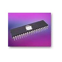
SST89V58RD2-33-C-NJE Microchip Technology, SST89V58RD2-33-C-NJE Datasheet - Page 28

SST89V58RD2-33-C-NJE
Manufacturer Part Number
SST89V58RD2-33-C-NJE
Description
IC MCU 8BIT 40KB FLASH 44PLCC
Manufacturer
Microchip Technology
Series
FlashFlex®r
Datasheet
1.SST89V54RD2-33-C-NJE.pdf
(77 pages)
Specifications of SST89V58RD2-33-C-NJE
Program Memory Type
FLASH
Program Memory Size
32KB (32K x 8)
Package / Case
44-LCC (J-Lead)
Core Processor
8051
Core Size
8-Bit
Speed
33MHz
Connectivity
EBI/EMI, SPI, UART/USART
Peripherals
Brown-out Detect/Reset, POR, WDT
Number Of I /o
36
Eeprom Size
8K x 8
Ram Size
1K x 8
Voltage - Supply (vcc/vdd)
2.7 V ~ 3.6 V
Oscillator Type
External
Operating Temperature
0°C ~ 70°C
Processor Series
SST89xxxRD
Core
8051
Data Bus Width
8 bit
Data Ram Size
1 KB
Interface Type
SPI, UART
Maximum Clock Frequency
33 MHz
Number Of Programmable I/os
32
Number Of Timers
3
Operating Supply Voltage
2.7 V to 3.6 V
Maximum Operating Temperature
+ 70 C
Mounting Style
SMD/SMT
Minimum Operating Temperature
0 C
Lead Free Status / RoHS Status
Lead free / RoHS Compliant
Data Converters
-
Lead Free Status / Rohs Status
Lead free / RoHS Compliant
Available stocks
Company
Part Number
Manufacturer
Quantity
Price
Company:
Part Number:
SST89V58RD2-33-C-NJE
Manufacturer:
Microchip Technology
Quantity:
10 000
Part Number:
SST89V58RD2-33-C-NJE
Manufacturer:
SST
Quantity:
20 000
Data Sheet
SPI Control Register (SPCR)
SPI Status Register (SPSR)
©2007 Silicon Storage Technology, Inc.
Location
Location
D5H
AAH
Symbol
SPIE
SPE
DORD
MSTR
CPOL
CPHA
SPR1, SPR0
Symbol
SPIF
WCOL
SPIE
SPIF
7
7
WCOL
SPE
6
Function
If both SPIE and ES are set to one, SPI interrupts are enabled.
SPI enable bit.
0: Disables SPI.
1: Enables SPI and connects SS#, MOSI, MISO, and SCK to pins P1.4, P1.5, P1.6, P1.7.
Data Transmission Order.
0: MSB first in data transmission.
1: LSB first in data transmission.
Master/Slave select.
0: Selects Slave mode.
1: Selects Master mode.
Clock Polarity
0: SCK is low when idle (Active High).
1: SCK is high when idle (Active Low).
Clock Phase control bit. The CPHA bit with the CPOL bit control the clock and data
relationship between master and slave. See Figures 6-5 and 6-6.
0: Shift triggered on the leading edge of the clock.
1: Shift triggered on the trailing edge of the clock.
SPI Clock Rate Select bits. These two bits control the SCK rate of the device
configured as master. SPR1 and SPR0 have no effect on the slave. The relationship
between SCK and the oscillator frequency, f
6
Function
SPI Interrupt Flag.
Upon completion of data transfer, this bit is set to 1.
If SPIE =1 and ES =1, an interrupt is then generated.
This bit is cleared by software.
Write Collision Flag.
Set if the SPI data register is written to during data transfer.
This bit is cleared by software.
SPR1
0
0
1
1
DORD
5
5
-
SPR0
0
1
0
1
MSTR
4
4
-
28
SCK = f
CPOL
3
3
SST89V54RD2/RD / SST89V58RD2/RD
-
OSC
128
16
64
4
divided by
CPHA
OSC
2
2
-
, is as follows:
SPR1
1
1
-
SPR0
FlashFlex MCU
0
0
-
S71255-10-000
Reset Value
Reset Value
00xxxxxxb
00H
12/07


