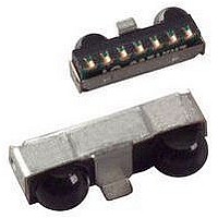
TFDU6103-TR3 Vishay, TFDU6103-TR3 Datasheet - Page 7

TFDU6103-TR3
Manufacturer Part Number
TFDU6103-TR3
Description
Infrared Transceivers SIR 115.2kbits Side View
Manufacturer
Vishay
Type
Fastr
Datasheet
1.TFDU6103-TR3.pdf
(13 pages)
Specifications of TFDU6103-TR3
Data Transmission Rate
4000 Kbits/s
Input Current
10 mA
Mounting Style
SMD/SMT
Power Dissipation
500 mW
Wavelength
886 nm
Continual Data Transmission
4 Mbit/s
Transmission Distance
1 m
Radiant Intensity
170 mW/sr
Half Intensity Angle Degrees
48 deg
Pulse Width
2.1 us
Maximum Rise Time
40 ns
Maximum Fall Time
40 ns
Led Supply Voltage
- 0.5 V to 6.5 V
Maximum Forward Current
10 mA
Operating Voltage
2.4 V to 5.5 V
Maximum Operating Temperature
+ 85 C
Minimum Operating Temperature
- 25 C
Dimensions
9.7 mm x 4.7 mm x 4 mm
Data Rate Max
4Mbps
Data Transmission Distance
1m
Peak Wavelength
886nm
Supply Current
2mA
Supply Voltage Range
2.4V To 5.5V
Operating Temperature Range
-25°C To +85°C
Msl
MSL 4 - 72 Hours
Data Rate
4Mbps
Angle Of Half Sensitivity
48°
Communication Distance
100
Package Type
Ultra Small Profile
Fall Time
40ns
Rise Time
40ns
Operating Supply Voltage (typ)
2.5/3.3/5V
Operating Supply Voltage (min)
2.4V
Operating Supply Voltage (max)
5.5V
Mounting
Surface Mount
Pin Count
8
Operating Temp Range
-25C to 85C
Operating Temperature Classification
Commercial
Idle Current, Typ @ 25° C
2mA
Link Range, Low Power
1m
Operating Temperature
-25°C ~ 85°C
Orientation
Side View
Shutdown
*
Size
9.7mm x 4.7mm x 4mm
Standards
IrPHY 1.4
Supply Voltage
2.4 V ~ 5.5 V
Lead Free Status / RoHS Status
Lead free / RoHS Compliant
Lead Free Status / RoHS Status
Lead free / RoHS Compliant, Lead free / RoHS Compliant
Available stocks
Company
Part Number
Manufacturer
Quantity
Price
Company:
Part Number:
TFDU6103-TR3
Manufacturer:
ST
Quantity:
1 001
Company:
Part Number:
TFDU6103-TR3
Manufacturer:
VISHAY
Quantity:
6 580
SETTING
MODE (2.4 kbit/s to 115.2 kbit/s)
1. Set SD input to logic “high”.
2. Set TXD input to logic “low”. Wait t
3. Set SD to logic “low” (this negative edge latches state of
4. TXD must be held for t
After that TXD is enabled as normal TXD input and the
transceiver is set for the lower bandwidth (9.6 kbit/s to
115.2 kbit/s) mode.
Note
When applying this sequence to the device already in the lower
bandwidth mode, the SD pulse is interpreted as shutdown. In this
case the RXD output of the transceiver may react with a single pulse
(going active low) for a duration less than 2 µs. The operating
software should take care for this condition.
In case the applied SD pulse is longer than 4 µs, no RXD pulse is to
be expected but the receiver startup time is to be taken into account
before the device is in receive condition.
RECOMMENDED SOLDER PROFILES
Solder Profile for Sn/Pb Soldering
Lead (Pb)-free, Recommended Solder Profile
The TFDU6103 is a lead (Pb)-free transceiver and qualified
for lead (Pb)-free processing. For lead (Pb)-free solder paste
like Sn
profiles: Ramp-Soak-Spike (RSS) and Ramp-To-Spike
(RTS). The Ramp-Soak-Spike profile was developed
Document Number: 81211
Rev. 1.4, 29-Jul-09
TABLE 2 - TRUTH TABLE
TXD, which determines speed setting).
Fig. 3 - Recommended Solder Profile for Sn/Pb soldering
High
Low
SD
19535
260
240
220
200
180
160
140
120
100
(3.0 - 4.0)
80
60
40
20
0
0
TO THE
Ag
2 to 4 °C/s
50
High > 150 µs
(0.5 - 0.9)
High
TXD
Low
Low
Low
100
x
Fast Infrared Transceiver Module (FIR, 4 Mbit/s)
irdasupportAM@vishay.com, irdasupportAP@vishay.com,
h
160 °C max.
Cu, there are two standard reflow
240 °C max.
120 to180 s
200 ns.
150
Time/s
For technical questions within your region, please contact one of the following:
LOWER BANDWIDTH
INPUTS
2 to 4 °C/s
OPTICAL INPUT IRRADIANCE mW/m
200
s
for 2.4 V to 5.5 V Operation
200 ns.
90 s max.
10 s max. at 230 °C
250
< max. irradiance E
> max. irradiance E
> min. irradiance E
300
< 4
x
x
x
350
e
e
e
primarily for reflow ovens heated by infrared radiation. With
widespread use of forced convection reflow ovens the
Ramp-To-Spike profile is used increasingly. Shown in
figure 4 and 5 are Vishay's recommended profiles for use
with the TFDU6103 transceivers. For more details please
refer to the application note “SMD Assembly Instructions”.
A ramp-up rate less than 0.9 °C/s is not recommended.
Ramp-up rates faster than 1.3 °C/s could damage an optical
part because the thermal conductivity is less than compared
to a standard IC.
Wave Soldering
For TFDUxxxx and TFBSxxxx transceiver devices wave
soldering is not recommended.
Manual Soldering
Manual soldering is the standard method for lab use.
However,
recommended because the risk of damage is highly
dependent on the experience of the operator. Nevertheless,
we added a chapter to the above mentioned application note,
describing manual soldering and desoldering.
2
SD
TXD
Weakly pulled (500 k) to V
irdasupportEU@vishay.com
Fig. 2 - Mode Switching Timing Diagram
for
50 %
Low (active)
Low (active)
a
RXD
High
High
x
production
Vishay Semiconductors
t
s
OUTPUTS
50 %
t
h
CC1
process
50 %
TFDU6103
TRANSMITTER
High: FIR
Low: SIR
it
www.vishay.com
I
0
0
0
0
0
cannot
e
14873
be
7


