MM232R FTDI, MM232R Datasheet - Page 7
MM232R
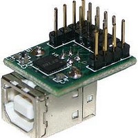
Manufacturer Part Number
MM232R
Description
Interface Modules & Development Tools USB to Serial UART Mini Dev Mod FT232R
Manufacturer
FTDI
Type
Development Moduler
Specifications of MM232R
Interface Type
USB, Serial, UART
Data Bus Width
Serial
Operating Supply Voltage
1.8 V to 5.25 V
Product
Interface Modules
Supported Devices
FT232RQ
Svhc
No SVHC (18-Jun-2010)
Development Tool Type
Development Kit
Kit Features
Single Chip USB To Asynchronous Serial Data Transfer Interface, Entire USB Protocol Handled
Rohs Compliant
Yes
Supported Families
FT232RQ
Tool / Board Applications
USB To Serial UART Converter
For Use With/related Products
FT232R
Lead Free Status / RoHS Status
Lead free / RoHS Compliant
Other names
626-DLP-MM232R


Document Reference No.: FT_000214
MM232R USB - Serial UART Development Module Incorporating Clock Generator
Datasheet Version 1.1
Clearance No.: FTDI# 132
Integrated Level Converter on UART Interface and Control Signals - VCCIO pin supply can be from
1.8V to 5V. Connecting the VCCIO pin to 1.8V, 2.8V, or 3.3V allows the device to directly interface to 1.8V,
2.8V or 3.3V and other logic families without the need for external level converter I.C. devices.
5V / 3.3V / 2.8V / 1.8V Logic Interface - The FT232R provides true CMOS Drive Outputs and TTL level
Inputs.
Integrated Power-On-Reset (POR) Circuit- The device incorporates an internal POR function. A RESET#
pin is available in order to allow external logic to reset the FT232R where required. However, for many
applications the RESET# pin can be left unconnected, or pulled up to VCCIO.
Lower Operating and Suspend Current - The device operating supply current has been further reduced
to 15mA, and the suspend current has been reduced to around 70μA. This allows greater margin for
peripheral designs to meet the USB suspend current limit of 500μA.
Low USB Bandwidth Consumption - The operation of the USB interface to the FT232R has been
designed to use as little as possible of the total USB bandwidth available from the USB host controller.
High Output Drive Option - The UART interface and CBUS I/O pins can be made to drive out at three
times the standard signal drive level thus allowing multiple devices to be driven, or devices that require
greater signal drive strength to be interfaced to the FT232R. This option is enabled in the internal EEPROM.
Power Management Control for USB Bus Powered, High Current Designs - The PWREN# signal can
be used to directly drive a transistor or P-Channel MOSFET in applications where power switching of
external circuitry is required. An option in the internal EEPROM makes the device gently pull down on its
UART interface lines when the power is shut off (PWREN# is high). In this mode any residual voltage on
external circuitry is bled to GND when power is removed, thus ensuring that external circuitry controlled by
PWREN# resets reliably when power is restored.
UART Pin Signal Inversion - The sense of each of the eight UART signals can be individually inverted by
setting options in the internal EEPROM. Thus, CTS# (active low) can be changed to CTS (active high), or
TXD can be changed to TXD#.
FTDIChip-ID™ - Each FT232R is assigned a unique number which is burnt into the device at manufacture.
This ID number cannot be reprogrammed by product manufacturers or end-users. This allows the possibility
of using FT232R based dongles for software licensing. Further to this, a renewable license scheme can be
implemented based on the FTDIChip-ID™ number when encrypted with other information. This encrypted
number can be stored in the user area of the FT232R internal EEPROM, and can be decrypted, then
compared with the protected FTDIChip-ID™ to verify that a license is valid. Web based applications can be
used to maintain product licensing this way. An application note describing this feature is available
separately from www.ftdichip.com.
Improved EMI Performance - The reduced operating current and improved on-chip VCC decoupling
significantly improves the ease of PCB design requirements in order to meet FCC, CE and other EMI related
specifications.
Programmable Receive Buffer Timeout - The receive buffer timeout is used to flush remaining data
from the receive buffer. This time defaults to 16ms, but is programmable over USB in 1ms increments from
1ms to 255ms, thus allowing the device to be optimised for protocols that require fast response times from
short data packets.
Baud Rates - The FT232R supports all standard baud rates and non-standard baud rates from 300 Baud up
to 3 Megabaud. Achievable non-standard baud rates are calculated as follows -Baud Rate = 3000000 / (n +
14
x) where „n‟ can be any integer between 2 and 16,384 (= 2
) and „x’ can be a sub-integer of the value 0,
0.125, 0.25, 0.375, 0.5, 0.625, 0.75, or 0.875. When n = 1, x = 0, i.e. baud rate divisors with values
between 1 and 2 are not possible. This gives achievable baud rates in the range 183.1 baud to 3,000,000
baud. When a non-standard baud rate is required simply pass the required baud rate value to the driver as
normal, and the FTDI driver will calculate the required divisor, and set the baud rate. See FTDI application
note AN232B-05 for more details.
Extended Operating Temperature Range - The FT232R operates over an extended temperature range
of -40º to +85º C thus allowing the device to be used in automotive and industrial applications.
New Package Options - The FT232R is available in two packages - a compact 28 pin SSOP (FT232RL) and
an ultra-compact 5mm x 5mm pinless QFN-32 package (FT232RQ). Both packages are lead ( Pb ) free, and
use a „green‟ compound. Both packages are fully compliant with European Union directive 2002/95/EC. The
MM232R module uses a FT232RQ device in its design.
6
© Copyright 2010 Future Technology Devices International Ltd
Related parts for MM232R
Image
Part Number
Description
Manufacturer
Datasheet
Request
R

Part Number:
Description:
Interface Modules & Development Tools USB to Serial UART MiniB Dev Mod FT232R
Manufacturer:
FTDI
Datasheet:

Part Number:
Description:
BOARD, EVALUATION, EU PSU
Manufacturer:
FTDI
Datasheet:
Part Number:
Description:
BOARD, EVALUATION, UK PSU
Manufacturer:
FTDI
Datasheet:
Part Number:
Description:
BOARD, EVALUATION, US PSU
Manufacturer:
FTDI
Datasheet:
Part Number:
Description:
Specifications: Manufacturer: FTDI ; Product Category: USB Interface IC ; RoHS: Details ; Operating Supply Voltage: 3 V to 5.25 V ; Supply Current: 25 mA ; Maximum Operating Temperature: + 70 C ; Mounting Style: SMD/SMT ; Package / Case: QFN-32
Manufacturer:
FTDI
Part Number:
Description:
integr. usb2.0/uart lqfp32 rohs ftdi reel c1k...
Manufacturer:
FTDI
Datasheet:
Part Number:
Description:
Interface Development Tools USB to UART Breakout Board
Manufacturer:
FTDI
Datasheet:

Part Number:
Description:
IC USB TO SERIAL UART 32-QFN
Manufacturer:
FTDI, Future Technology Devices International Ltd

Part Number:
Description:
USB Interface IC USB to Serial UART Enhanced IC SSOP-28
Manufacturer:
FTDI
Datasheet:

Part Number:
Description:
IC, USB UART INTERFACE, SSOP-28
Manufacturer:
FTDI
Datasheet:

Part Number:
Description:
IC, USB UART INTERFACE, QFN-32
Manufacturer:
FTDI
Datasheet:
Part Number:
Description:
IC, USB FIFO INTERFACE, SSOP-28
Manufacturer:
FTDI
Datasheet:
Part Number:
Description:
MODULE, USB, 4 PORT, FT4232H BASED
Manufacturer:
FTDI
Datasheet:
Part Number:
Description:
357-036-542-201 CARDEDGE 36POS DL .156 BLK LOPRO
Manufacturer:
FTDI
Datasheet:
Part Number:
Description:
357-036-542-201 CARDEDGE 36POS DL .156 BLK LOPRO
Manufacturer:
FTDI
Datasheet: