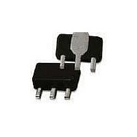
AH125-89PCB900 TriQuint, AH125-89PCB900 Datasheet - Page 11

AH125-89PCB900
Manufacturer Part Number
AH125-89PCB900
Description
RF Modules & Development Tools .4-2.7GHz Eval Board
Manufacturer
TriQuint
Datasheet
1.AH125-89PCB2140.pdf
(12 pages)
Specifications of AH125-89PCB900
Board Size
4.25 mm x 4.6 mm x 1.6 mm
Minimum Frequency
400 MHz
Minimum Operating Temperature
- 40 C
Supply Voltage (min)
5 V
Product
RF Modules
Maximum Frequency
3.6 GHz
Supply Voltage (max)
6 V
Supply Current
170 mA
Maximum Operating Temperature
+ 85 C
For Use With/related Products
AH125
Lead Free Status / RoHS Status
Lead free / RoHS Compliant
Other names
1071315
Application Note
½W High Linearity InGaP HBT Amplifier
Frequency
Gain
Input Return Loss
Output Return Loss
EVM
Output P1dB
Output IP3
Pout=+16 dBm/tone, 1MHz spacing
Quiescent Current, Icq
Vcc
Note: This reference design was constructed on FR4 to illustrate potential AH125 performance in the 3.4-3.6 GHz frequency range. For customer applications
of AH125 at these frequencies, we recommend the use of more suitable materials such as Rogers 3000 series.
TriQuint Semiconductor, Inc • Phone 503-615-9000 • FAX: 503-615-8900 • e-mail: info-sales@tqs.com • Web site: www.TriQuint.com
Circuit Board Material: 0.014” FR4, single layer, 1 oz copper, ε
Microstrip line details: width = .031”, spacing = .035”
Pout=+18 dBm
Typical O-FDMA Performance at 25°C
13
12
10
11
190
180
170
160
150
140
9
8
3.30
10
T
T
LEAD
LEAD
=+25°C
=+25°C
C1
12
3.40
3.4 GHz
Current vs Output Power
Gain vs. Frequency
14
R1
Output Power (dBm)
Frequency (GHz)
C10
+49.5 +45.7 45.2
11.5
802.16-2004 O-FDMA, 64QAM-1/2, 1024-FFT, 20 symbols and 30 subchannels, 5 MHz Carrier BW
+27
3.4
1.1
16
8
3.50
3.5 GHz
16
C3
C8
C4
C9
+27.3 +27.5 dBm
12.1
150
3.5
1.0
15
13
+5
C8
18
R2
3.60
3.6 GHz
C2
3.6
1.1
12
21
11
20
r
3.4-3.6 GHz Reference Design
= 4.3,
3.70
GHz
dBm
mA
22
dB
dB
dB
%
V
-10
-15
-20
-25
-30
20
15
10
-5
5
0
0
3.30
10
Notes:
1.
2.
3.
4.
5.
6.
T
T
LEAD
LEAD
=+25°C
=+25°C
The primary RF microstrip line is 50
Components shown on the silkscreen but not on the schematic are not used.
0
The edge of C9 is placed at 60 mil from AH125 RFout pin. (11.6
The edge of C10 is placed at 45 mil from AH125 RFin pin. (8.7
The edge of L2 is placed next to the edge of C10.
12
S11
Ω
3.40
jumpers can be replaced with copper trace in target application.
Return Loss vs. Frequency
Efficiency vs Output Power
S22
14
Output Power (dBm)
Frequency (GHz)
3.4 GHz
3.50
16
3.5 GHz
18
3.60
20
3.6 GHz
3.70
22
Ω
Specifications and information are subject to change without notice
.
55
50
45
40
35
5
4
3
2
1
0
12
10
802.16-2004 O-FDMA, 64QAM-
1/2, 1024-FFT, 20 symbols and 30
subchannels, 5 MHz Carrier BW
T
1 MHz tone spacing
LEAD
=+25°C
12
14
OIP3 vs. Output Power/Tone
3.4 GHz
Output Power/Tone (dBm)
EVM vs. Output Power
14
Output Power (dBm)
o
o
@ 3.5 GHz)
3.5 GHz
@ 3.5 GHz)
3.4 GHz
16
16
Page 11 of 12 April 2010
18
3.5 GHz
3.6 GHz
T
LEAD
18
=+25°C
20
3.6 GHz
22
20


