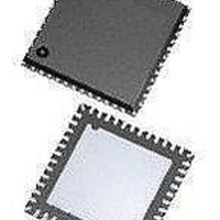
ASD5010L500INT Arctic Silicon Devices, ASD5010L500INT Datasheet - Page 16

ASD5010L500INT
Manufacturer Part Number
ASD5010L500INT
Description
ADC (A/D Converters) A-D Conv, Dig Gain Dual 8 bit 500MSPS
Manufacturer
Arctic Silicon Devices
Datasheet
1.ASD5010L500INT.pdf
(35 pages)
Specifications of ASD5010L500INT
Number Of Converters
2
Number Of Adc Inputs
4
Conversion Rate
500 MSPs
Resolution
8 bit
Snr
49.5 dB
Voltage Reference
1 V
Supply Voltage (max)
2 V
Supply Voltage (min)
1.7 V
Maximum Power Dissipation
295 mW
Maximum Operating Temperature
+ 85 C
Mounting Style
SMD/SMT
Package / Case
QFN-48
Input Voltage
1.8 V
Minimum Operating Temperature
- 40 C
Lead Free Status / RoHS Status
Lead free / RoHS Compliant
Preliminary Product Specification
Undefined register addresses must not be written to; incorrect behavior may be the result.
Unused register bits (blank table cells) must be set to '0' when programming the registers.
All registers can be written to while the chip is in power down mode.
*) These registers requires a power down cycle when written to (See Start up Initialization).
ASD5010
cgain1_ch1 <3:0>
jitter_ctrl<7:0>
channel_num <2:0>
*
clk_divide<1:0>*
coarse_gain_cfg
fine_gain_en
fgain_branch1<6:0> Programmable fine gain for branch1.
fgain_branch2<6:0> Programmable fine gain for branch 2.
fgain_branch3<6:0> Programmable fine gain for branch 3.
fgain_branch4<6:0> Programmable fine gain for branch 4.
fgain_branch5<6:0> Programmable fine gain for branch 5.
fgain_branch6<6:0> Programmable fine gain for branch 6.
fgain_branch7<6:0> Programmable fine gain for branch 7.
fgain_branch8<6:0> Programmable fine gain for branch 8.
inp_sel_adc1<4:0>
inp_sel_adc2<4:0>
inp_sel_adc3<4:0>
inp_sel_adc4<4:0>
phase_ddr<1:0>
pat_deskew
pat_sync
btc_mode
msb_first
adc_curr<2:0>
ext_vcm_bc<1:0>
lvds_pd_mode
low_clk_freq *
lvds_advance
lvds_delay
fs_cntrl<5:0>
startup_ctrl<2:0> *
Name
in a Dual Channel setup.
Programmable coarse gain channel 1
in a Single Channel setup.
Clock jitter adjustment.
Set number of channels: 1, 2 or 4
channels.
Define clock divider factor: 1, 2, 4 or 8
Configures the coarse gain setting
Enable use of fine gain.
Input select for adc 1.
Input select for adc 2.
Input select for adc 3.
Input select for adc 4.
Controls the phase of the LCLK
output relative to data.
Enable deskew pattern mode.
Enable sync pattern mode.
Binary two's complement format for
ADC output data.
Serialized ADC output data comes out
with MSB first.
ADC current scaling.
VCM buffer driving strength control.
Controls LVDS power down mode
Low clock frequency used.
Advance LVDS data bits and frame
clock by one clock cycle
Delay LVDS data bits and frame clock
by one clock cycle
Fine adjust ADC full scale range
Controls start-up time.
Description
Signal input: IP1/IN1
Signal input: IP2/IN2
Signal input: IP3/IN3
Signal input: IP4/IN4
Straight offset binary
x-gain enabled
rev 2.0, 2010.11.08
High z-mode
Divide by 1
90 degrees
0% change
4 channels
160 fsrms
0dB gain
0dB gain
0dB gain
0dB gain
0dB gain
0dB gain
0dB gain
0dB gain
Default
Disabled
LSB first
Nominal
Nominal
Inactive
Inactive
Inactive
Inactive
Inactive
1x gain
Page 16 of 35
'000'
D15 D14D13D12D11D10 D9 D8 D7 D6 D5 D4 D3 D2 D1 D0
X
X
X
X
X
X
X
X
X
X
X
X
X
X
X
X
X
X
X
X
X
X X X
X X X
X X X
X X X
X X X
X X 0
X X 0
X X
X X X X X X X X
X X X X X X X
X X X X X X X
X X X X X X X
X X X X X X X
X X
X X
X 0
X X X X X X
0 X
X X X X 0
X X X X 0
X
X 0 0 0
X X X
X
X X X
0 0 0
0 0 0
X X X
X
0 X
X 0
Confidential
X
X
Address
0x30
0x31
0x33
0x34
0x35
0x36
0x37
0x3A
0x3B
0x42
0x45
0x46
0x50
0x52
0x53
0x55
0x56
Hex


