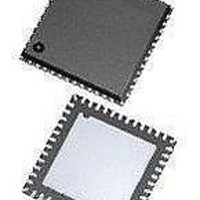
ASD5010L500INT Arctic Silicon Devices, ASD5010L500INT Datasheet - Page 26

ASD5010L500INT
Manufacturer Part Number
ASD5010L500INT
Description
ADC (A/D Converters) A-D Conv, Dig Gain Dual 8 bit 500MSPS
Manufacturer
Arctic Silicon Devices
Datasheet
1.ASD5010L500INT.pdf
(35 pages)
Specifications of ASD5010L500INT
Number Of Converters
2
Number Of Adc Inputs
4
Conversion Rate
500 MSPs
Resolution
8 bit
Snr
49.5 dB
Voltage Reference
1 V
Supply Voltage (max)
2 V
Supply Voltage (min)
1.7 V
Maximum Power Dissipation
295 mW
Maximum Operating Temperature
+ 85 C
Mounting Style
SMD/SMT
Package / Case
QFN-48
Input Voltage
1.8 V
Minimum Operating Temperature
- 40 C
Lead Free Status / RoHS Status
Lead free / RoHS Compliant
Preliminary Product Specification
PCB traces. This may result in reflections back to the LVDS outputs and loss of signal integrity. This effect can be
mitigated by enabling an internal termination between the positive and negative outputs of each LVDS buffer. Internal
termination mode can be selected by setting the en_lvds_term bit to '1'. Once this bit is set, the internal termination
values for the bit clock, frame clock, and data buffers can be independently programmed using sets of three bits. Table
19 shows how the internal termination of the LVDS buffers are programmed. The values are typical values and can vary
by up to ±20% from device to device and across temperature.
ASD5010
Table 19: LVDS output internal termination for LCLK, FCLK and data
term_*<2:0>
000
001
010
011
100
101
110
111
rev 2.0, 2010.11.08
Page 26 of 35
LVDS Internal Termination
Termination disabled
260
150
125
94
80
66
55
Confidential


