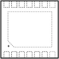
DS4402N+ Maxim Integrated Products, DS4402N+ Datasheet - Page 7

DS4402N+
Manufacturer Part Number
DS4402N+
Description
DAC (D/A Converters) IC DAC 2CH I2C ADJ justable Sink-Source
Manufacturer
Maxim Integrated Products
Datasheet
1.DS4402NTR.pdf
(9 pages)
Specifications of DS4402N+
Resolution
5 bit
Interface Type
Serial (I2C)
Supply Voltage (max)
5.5 V
Supply Voltage (min)
2.7 V
Maximum Operating Temperature
+ 85 C
Mounting Style
SMD/SMT
Minimum Operating Temperature
- 40 C
Number Of Converters
2
Package / Case
TDFN EP
Lead Free Status / RoHS Status
Lead free / RoHS Compliant
Acknowledgement (ACK and NACK): An Acknowledge-
ment (ACK) or Not Acknowledge (NACK) is always the
ninth bit transmitted during a byte transfer. The device
receiving data (the master during a read or the slave
during a write operation) performs an ACK by transmit-
ting a zero during the ninth bit. A device performs a
NACK by transmitting a one during the ninth bit. Timing
for the ACK and NACK is identical to all other bit writes
(Figure 4). An ACK is the acknowledgment that the
device is properly receiving data. A NACK is used to
terminate a read sequence or as an indication that the
device is not receiving data.
Byte Write: A byte write consists of 8 bits of information
transferred from the master to the slave (most significant
bit first) plus a 1-bit acknowledgement from the slave to
the master. The 8 bits transmitted by the master are
done according to the bit-write definition, and the
acknowledgement is read using the bit-read definition.
Byte Read: A byte read is an 8-bit information transfer
from the slave to the master plus a 1-bit ACK or NACK
from the master to the slave. The 8 bits of information
that are transferred (most significant bit first) from the
slave to the master are read by the master using the bit
read definition above, and the master transmits an ACK
using the bit write definition to receive additional data
bytes. The master must NACK the last byte read to ter-
minated communication so the slave will return control
of SDA to the master.
Slave Address Byte: Each slave on the I
responds to a slave address byte sent immediately follow-
ing a START condition. The slave address byte contains
Figure 3. I
SDA
SCL
NOTE: TIMING IS REFERENCED TO V
Two/Four-Channel, I
STOP
2
C Timing Diagram
t
BUF
START
t
HD:STA
IL(MAX)
t
LOW
AND V
IH(MIN)
t
R
.
t
HD:DAT
_____________________________________________________________________
t
HIGH
2
t
F
C bus
2
t
SU:DAT
C Adjustable Current DAC
the slave address in the most significant 7 bits and the
R/W bit in the least significant bit. The DS4402/DS4404s’
slave address is determined by the state of the A0 and A1
address pins. Table 1 describes the addresses corre-
sponding to the state of A0 and A1.
When the R/W bit is 0 (such as in A0h), the master is
indicating it will write data to the slave. If R/W = 1 (A1h
in this case), the master is indicating it wants to read
from the slave. If an incorrect slave address is written,
the DS4402/DS4404 assume the master is communi-
cating with another I
nication until the next START condition is sent.
Memory Address: During an I
master must transmit a memory address to identify the
memory location where the slave is to store the data.
The memory address is always the second byte trans-
mitted during a write operation following the slave
address byte.
Writing to a Slave: The master must generate a START
condition, write the slave address byte (R/W = 0), write
the memory address, write the byte of data, and gener-
ate a STOP condition. Remember that the master must
read the slave’s acknowledgement during all byte-write
operations.
Reading from a Slave: To read from the slave, the
master generates a START condition, writes the slave
address byte with R/W = 1, reads the data byte with a
NACK to indicate the end of the transfer, and generates
a STOP condition.
REPEATED
START
t
SU:STA
t
HD:STA
2
C device and ignore the commu-
I
2
t
SP
2
C Communication
C write operation, the
t
SU:STO
7


