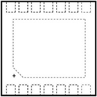
DS4402N+ Maxim Integrated Products, DS4402N+ Datasheet - Page 8

DS4402N+
Manufacturer Part Number
DS4402N+
Description
DAC (D/A Converters) IC DAC 2CH I2C ADJ justable Sink-Source
Manufacturer
Maxim Integrated Products
Datasheet
1.DS4402NTR.pdf
(9 pages)
Specifications of DS4402N+
Resolution
5 bit
Interface Type
Serial (I2C)
Supply Voltage (max)
5.5 V
Supply Voltage (min)
2.7 V
Maximum Operating Temperature
+ 85 C
Mounting Style
SMD/SMT
Minimum Operating Temperature
- 40 C
Number Of Converters
2
Package / Case
TDFN EP
Lead Free Status / RoHS Status
Lead free / RoHS Compliant
Using the typical circuit, assuming a typical output volt-
age of 2.0V, a feedback voltage of 0.8V, R1 = 500Ω,
and R2 = 333Ω, to adjust or margin the supply 20%
requires a full-scale current equal to [(0.2 x 2.0V) /
500Ω = 800µA]. Using Equation 1, R
ed [R
rent DAC in this configuration allows the output voltage
to be stepped linearly from 1.6V to 2.4V using 63 set-
tings. This corresponds to a resolution of 12.7mV/step.
The feedback voltage for adjustable power supplies
must be between 0.5V and V
DS4404 to properly sink/source currents for adjusting
the voltage.
In addition to defining the I
DS4404 address select inputs have an alternate function.
Two/Four-Channel, I
Figure 4. I
TRANSISTOR COUNT: 10,992
8
TYPICAL I
START
A)
B)
EXAMPLE I
______________________________________________________________________
SINGLE BYTE WRITE
-WRITE RESISTOR
SINGLE BYTE READ
-READ RESISTOR F8h
F9h TO 00h
FS
MSB
2
a7
C WRITE TRANSACTION
= (V
2
2
C TRANSACTIONS (WHEN A0 AND A1 ARE N.C.)
C Communication Examples
a6
REF
Power-Supply Feedback Voltage
for an Adjustable Power Supply
a5
Applications Information
ADDRESS*
/ 800µA) x (31 / 4) = 11.9kΩ]. The cur-
I
SLAVE
2
START
START
a4
C Reset on Address Change
a3
1 0 1 0 0 0 0 0
1 0 1 0 0 0 0 0
a2
2
A0h
A0h
C slave address, the DS4402/
Example Calculations
Chip Information
a1
CC
READ/
WRITE
R/W
LSB
- 0.5V for the DS4402/
SLAVE
SLAVE
ACK
ACK
SLAVE
FS
ACK
1 1 1 1 1 0 0 1
1 1 1 1 1 0 0 0
can be calculat-
MSB
F9h
F8h
b7
b6
REGISTER/MEMORY ADDRESS
2
SLAVE
SLAVE
*THE SLAVE ADDRESS IS DETERMINED BY ADDRESS PINS A0 AND A1 (SEE TABLE 1).
b5
ACK
ACK
C Adjustable Current DAC
b4
0 0 0 0 0 0 0 0
REPEATED
START
b3
b2
Changing the address select inputs resets the I
face. This function aborts the current transaction and puts
the SDA driver into a high-impedance state. This hard-
ware reset function should never be required because it
is achievable through software, but it does provide an
alternative way of resetting the I
To achieve the best results when using the DS4402/
DS4404, decouple the power supply with a 0.01µF or
0.1µF capacitor. Use a high-quality ceramic surface-
mount capacitor if possible. Surface-mount compo-
nents minimize lead inductance, which improves
performance, and ceramic capacitors tend to have
adequate high-frequency response for decoupling
applications.
Care should be taken to ensure that traces underneath
the DS4402/DS4404 do not short with the exposed pad.
The exposed pad should be connected to the signal
ground, or can be left unconnected.
For the latest package outline information and land patterns, go
to www.maxim-ic.com/packages.
PACKAGE TYPE
1 0 1 0 0 0 0 1
b1
SLAVE
ACK
14 TDFN-EP
A1h
LSB
b0
STOP
SLAVE
ACK
SLAVE
ACK
MSB
b7
b6
DATA
PACKAGE CODE
Package Information
b5
T1433+1
b4
Layout Considerations
DATA
MASTER
NACK
b3
2
C interface, if needed.
b2
STOP
V
b1
CC
DOCUMENT NO.
LSB
b0
Decoupling
21-0137
SLAVE
ACK
2
C inter-
STOP


