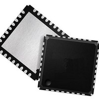
73M1906B-IVT/F Maxim Integrated Products, 73M1906B-IVT/F Datasheet - Page 4

73M1906B-IVT/F
Manufacturer Part Number
73M1906B-IVT/F
Description
Interface - Specialized DAA-FXO VolP SYSTEM HOST SIDE
Manufacturer
Maxim Integrated Products
Type
MicroDAA with PCM Highwayr
Datasheet
1.73M1866B-KEYCHN.pdf
(88 pages)
Specifications of 73M1906B-IVT/F
Operating Supply Voltage
3.3 V
Maximum Operating Temperature
+ 85 C
Minimum Operating Temperature
- 40 C
Mounting Style
SMD/SMT
Package / Case
QFN-32
Lead Free Status / RoHS Status
Lead free / RoHS Compliant
Available stocks
Company
Part Number
Manufacturer
Quantity
Price
Company:
Part Number:
73M1906B-IVT/F
Manufacturer:
LT
Quantity:
121
73M1866B/73M1966B Data Sheet
DS_1x66B_001
Figures
Figure 1: Simple 73M1x66B Reference Block Diagram ............................................................................ 6
Figure 2: 73M1906B 20-Pin TSSOP Pinout .............................................................................................. 8
Figure 3: 73M1916 20-Pin TSSOP Pinout ................................................................................................ 9
Figure 4: 73M1906B 32-Pin QFN Pinout ................................................................................................ 10
Figure 5: 73M1916 32-Pin QFN Pinout .................................................................................................. 12
Figure 6: 73M1866B 42-Pin Pinout ........................................................................................................ 14
Figure 7: SPI Timing Diagram ................................................................................................................ 18
Figure 8: PCM Timing Diagram for Positive Edge Transmit Mode and Negative Edge Receive Mode ..... 19
Figure 9: PCM Timing Diagram for Negative Edge Transmit Mode and Positive Edge Receive Mode ..... 20
Figure 10: Frequency Response of the Call Progress Monitor Filter ....................................................... 21
Figure 11: Demo Board Circuit Connecting AOUT to a Speaker ............................................................. 21
Figure 12: Recommended Circuit for the 73M1966B .............................................................................. 28
Figure 13: Recommended Circuit for the 73M1866B .............................................................................. 29
Figure 14: Suggested Over-Voltage Protection and EMI Suppression Circuit ......................................... 31
Figure 15: Daisy-Chain Configuration .................................................................................................... 34
Figure 16: SPI Write Operation – 8-bit Mode .......................................................................................... 34
Figure 17: SPI Read Transaction – 8-bit Mode ....................................................................................... 35
Figure 18: SPI Write Transaction – 16-bit Mode ..................................................................................... 35
Figure 19: SPI Read Transaction – 16-bit Mode ..................................................................................... 35
Figure 20: 8-bit Transmission Example .................................................................................................. 45
Figure 21: 16-bit Transmission Example ................................................................................................ 46
Figure 22: Example of PCM Highway Interconnect ................................................................................. 46
Figure 23: Example of PCM Highway Interconnect for Typical Large Systems ....................................... 46
Figure 24: Mapping of A-law Code to 16-bit Code .................................................................................. 48
Figure 25: Mapping of μ-law Code to 16-bit Code .................................................................................. 48
Figure 26: Transmit Path Overall Frequency Response to Fs of 8 kHz ................................................... 49
Figure 27: Transmit Path Passband Response for an 8 kHz Sample Rate .............................................. 49
Figure 28: Transmit Spectrum to 32 kHz for an 8 kHz Sample Rate ....................................................... 50
Figure 29: Overall Frequency Response of the Receive Path ................................................................. 51
Figure 30: Pass-band Response of the Overall Receive Path ................................................................. 51
Figure 31: Timing Relationships with Various TTS, TCS, TPOL, and RTS, RCS, RPOL Settings ............ 59
Figure 32: Line-Side Device AC and DC Circuits .................................................................................... 63
Figure 33: DC-IV Characteristics ............................................................................................................ 64
Figure 34: Tip-Ring Voltage versus Current Using Different DCIV Settings ............................................. 65
Figure 35: Voltage versus Current in the Seize Mode is the Same for All DCIV Settings ......................... 66
Figure 36: Magnitude Response of Impedance Matching Filter, ACZ (3:0)=0010 (ES 203 021-2) ........... 67
Figure 37: Magnitude Response of Billing Tone Notch Filter .................................................................. 67
Figure 38: Trans-hybrid Cancellation ..................................................................................................... 68
Figure 39: Loopback Modes Highlighted ................................................................................................ 78
Figure 40: Variation of Transmit Gain Digital Input to Analog Output at the Line ..................................... 80
Figure 41: Gain versus Frequency for Digital Input to Analog Output at the Line ..................................... 81
Figure 42: Signal to Total Distortion versus Input Level for Digital Input to Analog Output to the Line ...... 81
Figure 43: Variation of Receiver Analog Gain at the Line to the Digital DX Output .................................. 82
Figure 44: Gain versus Frequency for Analog Input at the Line to the Digital DX Output ......................... 83
Figure 45: Signal to Total Distortion versus Input Level for Analog at the Line to the Digital DX Output ... 83
Figure 46: Return Loss, @ 80 mA .......................................................................................................... 84
Figure 47: 20-Pin TSSOP Package Dimensions ..................................................................................... 85
Figure 48: 32-Pin QFN Package Dimensions ......................................................................................... 85
Figure 49: 42-Pin QFN Package Dimensions ......................................................................................... 86
4
Rev. 1.6


