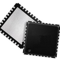
73M1906B-IVT/F Maxim Integrated Products, 73M1906B-IVT/F Datasheet - Page 43

73M1906B-IVT/F
Manufacturer Part Number
73M1906B-IVT/F
Description
Interface - Specialized DAA-FXO VolP SYSTEM HOST SIDE
Manufacturer
Maxim Integrated Products
Type
MicroDAA with PCM Highwayr
Datasheet
1.73M1866B-KEYCHN.pdf
(88 pages)
Specifications of 73M1906B-IVT/F
Operating Supply Voltage
3.3 V
Maximum Operating Temperature
+ 85 C
Minimum Operating Temperature
- 40 C
Mounting Style
SMD/SMT
Package / Case
QFN-32
Lead Free Status / RoHS Status
Lead free / RoHS Compliant
Available stocks
Company
Part Number
Manufacturer
Quantity
Price
Company:
Part Number:
73M1906B-IVT/F
Manufacturer:
LT
Quantity:
121
DS_1x66B_001
7.5
Three user-defined I/O pins are provided in the 32-pin QFN package of the 73M1966B only. The pins are
GPIO7, GPIO6 and GPIO5.
Each pin can be configured independently as either an input or an output by writing to the corresponding
I/O Direction (DIR) register.
At power on and after a reset, the GPIO pins are initialized to a high impedance state to avoid unwanted
current contention and consumption. The input structures are protected from floating inputs, and no
output levels are driven by any of the GPIO pins.
The mapping of GPIO pins is designed to correspond to the bit location in their control and status
registers.
The 73M1x66B supports the ability to generate an interrupt on the INT pin. The source can be configured
to generate on a rising or a trailing edge. Only GPIO ports that are configured as inputs can be used to
generate interrupts.
Rev. 1.6
Function
Mnemonic
DIR
GPIOn
ENGPIOn
POLn
GPIO pins are not available on the 20-pin package of the 73M1966B.
GPIO pins are not available on the 42-pin package of the 73M1866B.
GPIO Registers
Register
Location
0x04[7:5]
0x03[7:5]
0x05[7:5]
0x06[7:5]
Type
W
W
W
W
GPIO Input/Output Select
These control bits are used to designate the GPIO pins as either
inputs or outputs.
0 = GPIO pin is defined as an output.
1 = GPIO pin is defined as an input. (Default)
GPIO State
These bits reflect the status of the GPIO7, GPIO6 and GPIO5 pins.
If the DIR bit is reset, reading this field returns the logical value of the
appropriate GPIOn pin as an input.
If the DIR bit is set, the pins output the logical value as written.
GPIO Enable
Each of the GPIO enable bits in this register enables the
corresponding GPIO bit as an edge-triggered interrupt source. If a
GPIO bit is set to one, an edge (which edge depends on the value in
the GIP register) of the corresponding GPIO pin will cause the INT pin
to go active low, and the edge detectors will be rearmed when the
GPIO data register is read.
GPIO Interrupt Edge Selection
Defines the interrupt source as being either on a rising or a falling
edge of the corresponding GPIO pin.
0 = A rising edge will trigger an interrupt from the corresponding pin.
(Default)
1 = A falling edge will trigger an interrupt from the corresponding pin.
Description
73M1866B/73M1966B Data Sheet
43


