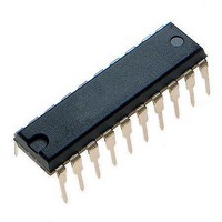
ATTINY461V-10PU Atmel, ATTINY461V-10PU Datasheet - Page 75

ATTINY461V-10PU
Manufacturer Part Number
ATTINY461V-10PU
Description
Microcontrollers (MCU) 4kB Flash 0.256kB EEPROM 16 I/O Pins
Manufacturer
Atmel
Specifications of ATTINY461V-10PU
Processor Series
ATTINY4x
Core
AVR8
Data Bus Width
8 bit
Data Ram Size
256 B
Interface Type
2-Wire/SPI/USI
Maximum Clock Frequency
10 MHz
Number Of Programmable I/os
16
Number Of Timers
2
Operating Supply Voltage
2.7 V to 5.5 V
Maximum Operating Temperature
+ 85 C
Mounting Style
Through Hole
Minimum Operating Temperature
- 40 C
On-chip Adc
11-ch x 10-bit
Program Memory Type
Flash
Program Memory Size
4 KB
Package / Case
PDIP-20
Package
20PDIP
Device Core
AVR
Family Name
ATtiny
Maximum Speed
10 MHz
Ram Size
256 Byte
Operating Temperature
-40 to 85 °C
Lead Free Status / RoHS Status
Lead free / RoHS Compliant
Available stocks
Company
Part Number
Manufacturer
Quantity
Price
Company:
Part Number:
ATTINY461V-10PU
Manufacturer:
ATMEL
Quantity:
6 223
- Current page: 75 of 242
- Download datasheet (5Mb)
11.5
2588E–AVR–08/10
Input Capture Unit
internal clock source, selected by the Clock Select bits (CS02:0). When no clock source is
selected (CS02:0 = 0) the timer is stopped. However, the TCNT0 value can be accessed by the
CPU, regardless of whether clk
counter clear or count operations. The Timer/Counter Overflow Flag (TOV0) is set when the
counter reaches the maximum value and it can be used for generating a CPU interrupt.
The Timer/Counter incorporates an Input Capture unit that can capture external events and give
them a time-stamp indicating time of occurrence. The external signal indicating an event, or mul-
tiple events, can be applied via the ICP0 pin or alternatively, via the analog-comparator unit. The
time-stamps can then be used to calculate frequency, duty-cycle, and other features of the sig-
nal applied. Alternatively the time-stamps can be used for creating a log of the events.
The Input Capture unit is illustrated by the block diagram shown in
the block diagram that are not directly a part of the Input Capture unit are gray shaded.
Figure 11-4. Input Capture Unit Block Diagram
The Output Compare Register OCR0A is a dual-purpose register that is also used as an 8-bit
Input Capture Register ICR0. In 16-bit Input Capture mode the Output Compare Register
OCR0B serves as the high byte of the Input Capture Register ICR0. In 8-bit Input Capture mode
the Output Compare Register OCR0B is free to be used as a normal Output Compare Register,
but in 16-bit Input Capture mode the Output Compare Unit cannot be used as there are no free
Output Compare Register(s). Even though the Input Capture register is called ICR0 in this sec-
tion, it is refering to the Output Compare Register(s).
When a change of the logic level (an event) occurs on the Input Capture pin (ICP0), alternatively
on the Analog Comparator output (ACO), and this change confirms to the setting of the edge
detector, a capture will be triggered. When a capture is triggered, the value of the counter
(TCNT0) is written to the Input Capture Register (ICR0). The Input Capture Flag (ICF0) is set at
ICP0
WRITE
OCR0B (8-bit)
TEMP (8-bit)
Comparator
Analog
ICR0 (16-bit Register)
ACO*
OCR0A (8-bit)
T0
is present or not. A CPU write overrides (has priority over) all
ACIC0*
DATA BUS
Canceler
Noise
ICNC0
(8-bit)
TCNT0H (8-bit)
TCNT0 (16-bit Counter)
Detector
Figure
ICES0
Edge
11-4. The elements of
TCNT0L (8-bit)
ICF0 (Int.Req.)
75
Related parts for ATTINY461V-10PU
Image
Part Number
Description
Manufacturer
Datasheet
Request
R

Part Number:
Description:
Manufacturer:
Atmel Corporation
Datasheet:

Part Number:
Description:
Manufacturer:
Atmel Corporation
Datasheet:

Part Number:
Description:
IC AVR MCU 4K 20MHZ 32-QFN
Manufacturer:
Atmel
Datasheet:

Part Number:
Description:
IC MCU AVR 4K FLASH 20MHZ 20SOIC
Manufacturer:
Atmel
Datasheet:

Part Number:
Description:
MCU AVR 4K FLASH 15MHZ 32-QFN
Manufacturer:
Atmel
Datasheet:

Part Number:
Description:
MCU AVR 4KB FLASH 15MHZ 32-VQFN
Manufacturer:
Atmel
Datasheet:

Part Number:
Description:
MCU AVR 4KB FLASH 20MHZ 20SOIC
Manufacturer:
Atmel
Datasheet:

Part Number:
Description:
IC MCU AVR 4K 20MHZ 32QFN
Manufacturer:
Atmel
Datasheet:

Part Number:
Description:
Microcontrollers (MCU) 4kB Flash 0.256kB EEPROM 16 I/O Pins
Manufacturer:
Atmel
Datasheet:

Part Number:
Description:
IC, MCU, 8BIT, 2K FLASH, 20SOIC
Manufacturer:
Atmel
Datasheet:


