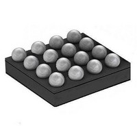
MAX15050EWE+T Maxim Integrated Products, MAX15050EWE+T Datasheet - Page 12

MAX15050EWE+T
Manufacturer Part Number
MAX15050EWE+T
Description
Switching Converters, Regulators & Controllers WLP 16 PIN 2.7MM egulator with Integr
Manufacturer
Maxim Integrated Products
Datasheet
1.MAX15050EWET.pdf
(15 pages)
Specifications of MAX15050EWE+T
Output Current
4 A
Input Voltage
2.9 V to 5.5 V
Switching Frequency
1 MHz
Operating Temperature Range
- 40 C to + 85 C
Mounting Style
SMD/SMT
Duty Cycle (max)
96 %
Package / Case
WLP-16
Lead Free Status / RoHS Status
Lead free / RoHS Compliant
The peak-to-peak inductor current (I
Use these equations for initial output-capacitor selec-
tion. Determine final values by testing a prototype or an
evaluation circuit. A smaller ripple current results in less
output-voltage ripple. Since the inductor ripple current
is a factor of the inductor value, the output-voltage rip-
ple decreases with larger inductance. Use ceramic
capacitors for low ESR and low ESL at the switching
frequency of the converter. The ripple voltage due to
ESL is negligible when using ceramic capacitors.
Load-transient response depends on the selected out-
put capacitance. During a load transient, the output
instantly changes by ESR x ∆I
troller can respond, the output deviates further,
depending on the inductor and output capacitor val-
ues. After a short time, the controller responds by regu-
lating the output voltage back to its predetermined
value. The controller response time depends on the
closed-loop bandwidth. A higher bandwidth yields a
faster response time, preventing the output from deviat-
ing further from its regulating value. See the Compen-
sation Design section for more details. The minimum
recommended output capacitance for the MAX15051
and MAX15051 is 47µF and 22µF, respectively.
When transitioning from skip mode to PWM mode
(MAX15050) with a large current load step, additional out-
put capacitance can be used to help minimize the load-
transient response. The input capacitor reduces the
current peaks drawn from the input power supply and
reduces switching noise in the device. The total input
capacitance must be equal to or greater than the value
given by the following equation to keep the input ripple
voltage within the specification and minimize the high-fre-
quency ripple current being fed back to the input source:
where V
voltage across the input capacitors and is recommend-
ed to be less than 2% of the minimum input voltage, D
is the duty cycle (V
(1/f
The impedance of the input capacitor at the switching fre-
quency should be less than that of the input source so
high-frequency switching currents do not pass through
the input source, but are instead shunted through the
input capacitor. The input capacitor must meet the ripple
High-Efficiency, 4A, 1MHz, Step-Down Regulators
with Integrated Switches in 2mm x 2mm Package
12
S
) = 1µs, and I
______________________________________________________________________________________
IN-RIPPLE
I
P P
C
−
IN MIN
OUT
is the maximum-allowed input ripple
_
=
OUT
V
IN
Input-Capacitor Selection
is the output load.
/V
f
=
S
−
IN
×
D x T x I
V
), T
OUT
V
L
IN RIPPLE
−
S
S
LOAD
is the switching period
x
V
OUT
P-P
OUT
V
IN
. Before the con-
) is:
current requirement imposed by the switching currents.
The RMS input ripple current is given by:
where I
The power transfer function consists of one double pole
and one zero. The double pole is introduced by the
inductor, L, and the output capacitor, C
output capacitor determines the zero. The double pole
and zero frequencies are given as follows:
where R
resistance (DCR) and the internal switch resistance,
R
output load resistance, which is equal to the rated output
voltage divided by the rated output current. ESR is the
total equivalent series resistance of the output capacitor. If
there is more than one output capacitor of the same type
in parallel, the value of the ESR in the above equation is
equal to that of the ESR of a single output capacitor divid-
ed by the total number of output capacitors.
The MAX15050/MAX15051 high switching frequency
allows the use of ceramic output capacitors. Since the ESR
of ceramic capacitors is typically very low, the frequency of
the associated transfer function zero is higher than the
unity-gain crossover frequency, f
used to compensate for the double pole created by the
output inductor and capacitor. The double pole produces
a gain drop of 40dB/decade and a phase shift of 180°. The
compensation network must compensate for this gain drop
and phase shift to achieve a stable high-bandwidth closed-
loop system. Therefore, use type III compensation as
shown in Figure 4 and Figure 5. Type III compensation
possesses three poles and two zeros with the first pole,
f
poles and zeros of the type III compensation are given by:
P1_EA
DS(ON)
f
P LC
1
, located at zero frequency (DC). Locations of other
_
I
RIPPLE
RIPPLE
L
. A typical value for R
is equal to the sum of the output inductor’s DC
=
f
P
2
f
=
is the input RMS ripple current.
Z ESR
_
LC
_
I
LOAD
f
f
Z
Z
1
2
=
_
_
2
EA
=
EA
π
×
2π
=
x L x C
=
V
2
OUT
2
x ESR x C
Compensation Design
π
π
DS(ON)
x R x C
x R x C
C
1
×
1
, and the zero cannot be
O
1
1
(
V
3
V
IN
1
IN
x
⎛
⎜
⎝
is 25mΩ. R
−
R
1
O
R
O
3
V
O
. The ESR of the
O
OUT
+
+
ESR
R
)
L
⎞
⎟
⎠
O
is the


