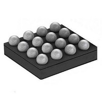
MAX15050EWE+T Maxim Integrated Products, MAX15050EWE+T Datasheet - Page 14

MAX15050EWE+T
Manufacturer Part Number
MAX15050EWE+T
Description
Switching Converters, Regulators & Controllers WLP 16 PIN 2.7MM egulator with Integr
Manufacturer
Maxim Integrated Products
Datasheet
1.MAX15050EWET.pdf
(15 pages)
Specifications of MAX15050EWE+T
Output Current
4 A
Input Voltage
2.9 V to 5.5 V
Switching Frequency
1 MHz
Operating Temperature Range
- 40 C to + 85 C
Mounting Style
SMD/SMT
Duty Cycle (max)
96 %
Package / Case
WLP-16
Lead Free Status / RoHS Status
Lead free / RoHS Compliant
The MAX15050/MAX15051 can soft-start into a prebi-
ased output without discharging the output capacitor.
In safe prebiased startup, both low-side and high-side
switches remain off to avoid discharging the prebiased
output. PWM operation starts when the voltage on
REFIN/SS crosses the voltage on FB. The PWM activity
starts with the low-side switch turning on first to build
the bootstrap capacitor charge. Power-good (PWRGD)
asserts 48 clock cycles after FB crosses 92.5% of the
final regulation set point. After 4096 clock cycles, the
MAX15050 switches from prebiased safe-startup mode
to either a skip mode or a forced PWM mode depend-
ing on whether the inductor current reaches zero. The
MAX15051 switches from the prebiased safe-startup
mode to forced PWM mode regardless of inductor cur-
rent level.
The MAX15051 also can start into a prebiased voltage
higher than the nominal set point without abruptly dis-
charging the output. This is achieved by using the sink
current control of the low-side MOSFET, which has four
internally set sinking current-limit thresholds. An internal
4-bit DAC steps through these thresholds, starting from
the lowest current limit to the highest, in 128 clock
cycles on every power-up.
High-Efficiency, 4A, 1MHz, Step-Down Regulators
with Integrated Switches in 2mm x 2mm Package
14
(BUMPS ON BOTTOM)
______________________________________________________________________________________
TOP VIEW
Soft-Starting Into a Prebiased Output
PWRGD
GND
BST
LX
A1
B1
C1
D1
MAX15050/MAX15051
GND
I.C.
LX
C2
A2
B2
FB
D2
WLP
Pin Configuration
COMP
I.C.
LX
A3
B3
C3
D3
IN
REFIN/SS
V
A4
EN
C4
D4
B4
IN
DD
Careful PCB layout is critical to achieve clean and sta-
ble operation. It is highly recommended to duplicate
the MAX15050/MAX15051 evaluation kit layout for opti-
mum performance. If deviation is necessary, follow
these guidelines for good PCB layout:
1) Place capacitors on IN, V
2) Keep the high-current paths as short and wide as
3) Connect IN, LX, and GND separately to a large
4) Ensure all feedback connections are short. Place
5) Route high-speed switching nodes, such as LX and
PROCESS: BiCMOS
For the latest package outline information and land patterns,
go to www.maxim-ic.com/packages. Note that a “+”, “#”, or
“-” in the package code indicates RoHS status only. Package
drawings may show a different suffix character, but the drawing
pertains to the package regardless of RoHS status.
PACKAGE
close as possible to the device and the corre-
sponding bump using direct traces.
possible. Keep the path of switching current short
and minimize the loop area formed by LX, the out-
put capacitors, and the input capacitors.
copper area to help cool the device to further
improve efficiency and long-term reliability.
the feedback resistors and compensation compo-
nents as close to the device as possible.
BST, away from sensitive analog areas (FB, COMP).
16 WLP
TYPE
PCB Layout Considerations and
PACKAGE
W162C2+1
CODE
Package Information
Thermal Performance
OUTLINE NO.
Chip Information
21-0200
DD
, and REFIN/SS as
PATTERN NO.
LAND
—


