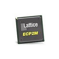
LFE2M20SE-5FN484C Lattice, LFE2M20SE-5FN484C Datasheet - Page 93

LFE2M20SE-5FN484C
Manufacturer Part Number
LFE2M20SE-5FN484C
Description
FPGA - Field Programmable Gate Array 19K LUTs 304 I/O S-Ser SERDES DSP -5
Manufacturer
Lattice
Datasheet
1.LFE2-12SE-6FN256C.pdf
(389 pages)
Specifications of LFE2M20SE-5FN484C
Number Of Macrocells
19000
Maximum Operating Frequency
311 MHz
Number Of Programmable I/os
304
Data Ram Size
1246208
Supply Voltage (max)
1.26 V
Maximum Operating Temperature
+ 85 C
Minimum Operating Temperature
0 C
Mounting Style
SMD/SMT
Supply Voltage (min)
1.14 V
Package / Case
FPBGA-484
Lead Free Status / RoHS Status
Lead free / RoHS Compliant
Available stocks
Company
Part Number
Manufacturer
Quantity
Price
Company:
Part Number:
LFE2M20SE-5FN484C
Manufacturer:
Lattice
Quantity:
135
Company:
Part Number:
LFE2M20SE-5FN484C
Manufacturer:
LATTICE
Quantity:
12
Company:
Part Number:
LFE2M20SE-5FN484C
Manufacturer:
Lattice Semiconductor Corporation
Quantity:
10 000
- Current page: 93 of 389
- Download datasheet (5Mb)
Lattice Semiconductor
SERDES High Speed Data Receiver (LatticeECP2M Family Only)
Table 3-11. Serial Input Data Specifications
Input Data Jitter Tolerance
A receiver’s ability to tolerate incoming signal jitter is very dependent on jitter type. High speed serial interface stan-
dards have recognized the dependency on jitter type and have recently modified specifications to indicate toler-
ance levels for different jitter types as they relate to specific protocols (e.g. FC, etc.). Sinusoidal jitter is considered
to be a worst case jitter type.
Table 3-12. Receiver Total Jitter Tolerance Specification
RX-CID
V
V
V
V
T
Z
RL
1. This is the number of bits allowed without a transition on the incoming data stream when using DC coupling.
2. This is the typical number of bit times to re-lock to a new phase of frequency within +/- 300 ppm, assuming 8b10b encoded data and the
3. AC coupling is used to interface to LVPECL and LVDS.
Deterministic
Random
Total
Deterministic
Random
Total
Deterministic
Random
Total
Deterministic
Random
Total
1. Values are measured with PRBS 2
2. Jitter specification is limited by measurement equipment capability.
RX-RELOCK
RX-TERM
RX-DIFF-S
RX-IN
RX-CM-DC
RX-CM-AC
Symbol
Description
CDR is in lock state. When CDR is in un-lock state, or reset is applied, the total re-lock settling time will be approximately 4ms including ana-
log settle time, calibration time, and acquisition time.
RX-RL
room temperature.
S
Stream of nontransitions
(CID = Consecutive Identical Digits) @ 10
Differential input sensitivity
Input levels
Input common mode range (DC coupled)
Input common mode range (AC coupled)
CDR re-lock time
Input termination 50/75 Ohm/High Z
Return loss (without package)
3.125 Gbps
2.5 Gbps
1.25 Gbps
250 Mbps
Frequency
2
2
600 mV differential eye
600 mV differential eye
600 mV differential eye
600 mV differential eye
600 mV differential eye
600 mV differential eye
600 mV differential eye
600 mV differential eye
600 mV differential eye
600 mV differential eye
600 mV differential eye
600 mV differential eye
Description
7
-1, all channels operating, FPGA Logic active, I/Os around SERDES pins quiet, voltages are nominal,
1
Condition
3
-12
BER
3-41
Min.
1
—
—
—
—
—
—
—
—
—
—
—
—
Min.
100
0.5
—
—
—
0
0
DC and Switching Characteristics
LatticeECP2/M Family Data Sheet
Typ.
7 @ 3.125 Gbps
20 @ 1.25 Gbps
—
—
—
—
—
—
—
—
—
—
—
—
Typ.
—
—
—
50
—
—
9
Max.
0.54
0.26
0.60
0.80
0.61
0.81
0.53
0.80
0.42
0.22
0.22
0.10
V
CCRX
Max.
3000
1.2
1.5
—
—
+ 0.8
UI, p-p
UI, p-p
UI, p-p
UI, p-p
UI, p-p
UI, p-p
UI, p-p
UI, p-p
UI, p-p
UI, p-p
UI, p-p
UI, p-p
Units
mV, p-p
Ohms
Units
Bits
Bits
dB
V
V
V
Related parts for LFE2M20SE-5FN484C
Image
Part Number
Description
Manufacturer
Datasheet
Request
R

Part Number:
Description:
FPGA - Field Programmable Gate Array 19K LUTs 140 I/O S-Ser SERDES DSP -5
Manufacturer:
Lattice
Datasheet:
Part Number:
Description:
FPGA LatticeECP2M Family 19000 Cells 90nm (CMOS) Technology 1.2V 484-Pin FBGA
Manufacturer:
LATTICE SEMICONDUCTOR
Datasheet:

Part Number:
Description:
FPGA LatticeECP2M Family 19000 Cells 90nm (CMOS) Technology 1.2V 256-Pin FBGA
Manufacturer:
Lattice
Datasheet:

Part Number:
Description:
IC FPGA 20KLUTS 140I/O 256-BGA
Manufacturer:
Lattice
Datasheet:

Part Number:
Description:
IC FPGA 20KLUTS 140I/O 256-BGA
Manufacturer:
Lattice
Datasheet:

Part Number:
Description:
IC FPGA 20KLUTS 304I/O 484-BGA
Manufacturer:
Lattice
Datasheet:

Part Number:
Description:
IC FPGA 19KLUTS 484FGPBGA
Manufacturer:
Lattice
Datasheet:

Part Number:
Description:
FPGA - Field Programmable Gate Array 19K LUTs 304 I/O S-Ser SERD DSP -6
Manufacturer:
Lattice

Part Number:
Description:
FPGA - Field Programmable Gate Array 19K LUTs 304 I/O S-Ser SERD DSP -7
Manufacturer:
Lattice

Part Number:
Description:
FPGA - Field Programmable Gate Array 19K LUTs 140 I/O S-Ser SERD DSP -6 I
Manufacturer:
Lattice

Part Number:
Description:
FPGA - Field Programmable Gate Array 19K LUTs 140 I/O S-Ser SERD DSP -6
Manufacturer:
Lattice

Part Number:
Description:
FPGA - Field Programmable Gate Array 19K LUTs 304 I/O S-Ser SERDES DSP -5
Manufacturer:
Lattice

Part Number:
Description:
FPGA - Field Programmable Gate Array 19K LUTs 304 I/O S-Ser SERD DSP -6 I
Manufacturer:
Lattice


