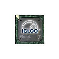
AGL060V5-VQG100 Actel, AGL060V5-VQG100 Datasheet - Page 97

AGL060V5-VQG100
Manufacturer Part Number
AGL060V5-VQG100
Description
FPGA - Field Programmable Gate Array 60K System Gates IGLOO
Manufacturer
Actel
Datasheet
1.AGL030V2-CSG81.pdf
(236 pages)
Specifications of AGL060V5-VQG100
Processor Series
AGL06
Core
IP Core
Maximum Operating Frequency
892.86 MHz
Number Of Programmable I/os
71
Data Ram Size
18432
Supply Voltage (max)
1.575 V
Maximum Operating Temperature
+ 70 C
Minimum Operating Temperature
0 C
Development Tools By Supplier
AGL-Icicle-Kit, AGL-Dev-Kit-SCS, Silicon-Explorer II, Silicon-Sculptor 3, SI-EX-TCA, FlashPro 4, FlashPro 3, FlashPro Lite
Mounting Style
SMD/SMT
Supply Voltage (min)
1.425 V
Number Of Gates
60 K
Package / Case
VQFP-100
Lead Free Status / RoHS Status
Lead free / RoHS Compliant
Available stocks
Company
Part Number
Manufacturer
Quantity
Price
Company:
Part Number:
AGL060V5-VQG100
Manufacturer:
Microsemi SoC
Quantity:
10 000
Company:
Part Number:
AGL060V5-VQG100I
Manufacturer:
Microsemi SoC
Quantity:
10 000
- Current page: 97 of 236
- Download datasheet (8Mb)
Figure 2-14 • B-LVDS/M-LVDS Multipoint Application Using LVDS I/O Buffers
Figure 2-15 • LVPECL Circuit Diagram and Board-Level Implementation
OUTBUF_LVPECL
R
T
Z
Z
Z
stub
0
0
Receiver
+
R
R
S
B-LVDS/M-LVDS
Bus LVDS (B-LVDS) and Multipoint LVDS (M-LVDS) specifications extend the existing LVDS standard to
high-performance multipoint bus applications. Multidrop and multipoint bus configurations may contain
any combination of drivers, receivers, and transceivers. Actel LVDS drivers provide the higher drive
current required by B-LVDS and M-LVDS to accommodate the loading. The drivers require series
terminations for better signal quality and to control voltage swing. Termination is also required at both
ends of the bus since the driver can be located anywhere on the bus. These configurations can be
implemented using the TRIBUF_LVDS and BIBUF_LVDS macros along with appropriate terminations.
Multipoint designs using Actel LVDS macros can achieve up to 200 MHz with a maximum of 20 loads. A
sample application is given in
section in
Example: For a bus consisting of 20 equidistant loads, the following terminations provide the required
differential voltage, in worst-case Industrial operating conditions, at the farthest receiver: R
R
LVPECL
Low-Voltage Positive Emitter-Coupled Logic (LVPECL) is another differential I/O standard. It requires
that one data bit be carried through two signal lines. Like LVDS, two pins are needed. It also requires
external resistor termination.
The full implementation of the LVDS transmitter and receiver is shown in an example in
building blocks of the LVPECL transmitter-receiver are one transmitter macro, one receiver macro, three
board resistors at the transmitter end, and one resistor at the receiver end. The values for the three driver
resistors are different from those used in the LVDS implementation because the output standard
specifications are different.
-
T
EN
R
Z
= 70 Ω, given Z
S
stub
FPGA
Z
Z
Table 2-148 on page 2-82
Z
0
0
stub
Transceiver
+
R
T
S
0
-
= 50 Ω (2") and Z
N
EN
P
R
Z
stub
S
Bourns Part Number: CAT16-PC4F12
100 Ω
100 Ω
Z
Z
Z
0
0
Figure
stub
Driver
+
R
D
and
S
2-14. The input and output buffer delays are available in the LVDS
stub
-
EN
R
Z
Table 2-149 on page
S
stub
187 W
= 50 Ω (~1.5").
R ev i si o n 1 8
Z
Z
Z
Z
Z
0
0
0
0
stub
= 50 Ω
= 50 Ω
Receiver
+
R
R
S
-
EN
100 Ω
R
Z
S
stub
2-82.
...
N
P
Z
Z
0
0
IGLOO Low Power Flash FPGAs
FPGA
Transceiver
+
–
+
R
T
S
-
EN
INBUF_LVPECL
R
S
Figure
S
BIBUF_LVDS
= 60 Ω and
Z
Z
2-15. The
0
0
2- 83
R
T
Related parts for AGL060V5-VQG100
Image
Part Number
Description
Manufacturer
Datasheet
Request
R

Part Number:
Description:
FPGA - Field Programmable Gate Array 60K System Gates IGLOO
Manufacturer:
Actel
Datasheet:

Part Number:
Description:
MCU, MPU & DSP Development Tools Silicon Sculptor Programming Mod
Manufacturer:
Actel

Part Number:
Description:
MCU, MPU & DSP Development Tools InSystem Programming ProASICPLUS Devices
Manufacturer:
Actel

Part Number:
Description:
Programming Socket Adapters & Emulators PQ160 Module
Manufacturer:
Actel

Part Number:
Description:
Programming Socket Adapters & Emulators Axcelerator Adap Module Kit
Manufacturer:
Actel

Part Number:
Description:
Programming Socket Adapters & Emulators Evaluation
Manufacturer:
Actel

Part Number:
Description:
Programming Socket Adapters & Emulators AFDX Solutions
Manufacturer:
Actel

Part Number:
Description:
Programming Socket Adapters & Emulators SILICON SCULPTOR ADAPTER MODULE
Manufacturer:
Actel
Datasheet:

Part Number:
Description:
Programming Socket Adapters & Emulators Axcelerator Adap Module Kit
Manufacturer:
Actel

Part Number:
Description:
Programming Socket Adapters & Emulators Evaluation
Manufacturer:
Actel


