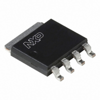
PSMN030-60YS,115 NXP Semiconductors, PSMN030-60YS,115 Datasheet - Page 9

PSMN030-60YS,115
Manufacturer Part Number
PSMN030-60YS,115
Description
MOSFET N-CH LFPAK
Manufacturer
NXP Semiconductors
Datasheet
1.PSMN030-60YS115.pdf
(15 pages)
Specifications of PSMN030-60YS,115
Input Capacitance (ciss) @ Vds
686pF @ 30V
Fet Type
MOSFET N-Channel, Metal Oxide
Fet Feature
Standard
Rds On (max) @ Id, Vgs
24.7 mOhm @ 15A, 10V
Drain To Source Voltage (vdss)
60V
Current - Continuous Drain (id) @ 25° C
29A
Vgs(th) (max) @ Id
4V @ 1mA
Gate Charge (qg) @ Vgs
13nC @ 10V
Power - Max
56W
Mounting Type
Surface Mount
Package / Case
SC-100, SOT-669
Configuration
Single
Transistor Polarity
N-Channel
Resistance Drain-source Rds (on)
49.6 mOhms
Drain-source Breakdown Voltage
54 V
Continuous Drain Current
21 A
Power Dissipation
56 W
Mounting Style
SMD/SMT
Lead Free Status / RoHS Status
Lead free / RoHS Compliant
Other names
568-5584-2
Available stocks
Company
Part Number
Manufacturer
Quantity
Price
Part Number:
PSMN030-60YS,115
Manufacturer:
NEXPERIA/安世
Quantity:
20 000
NXP Semiconductors
PSMN030-60YS
Product data sheet
Fig 13. Drain-source on-state resistance as a function
Fig 15. Gate-source voltage as a function of gate
R
(mΩ)
DSon
V
(V)
GS
70
50
30
10
10
8
6
4
2
0
of drain current; typical values
charge; typical values
0
0
12V
V
5
GS
(V) = 4.5
48V
10
10
I
D
(A)
V
Q
All information provided in this document is subject to legal disclaimers.
DS
003aae125
003aae123
G
(nC)
5
= 30V
5.5
6.5
10
6
8
Rev. 02 — 25 October 2010
20
15
N-channel LFPAK 60 V 24.7 mΩ standard level MOSFET
Fig 14. Gate charge waveform definitions
Fig 16. Input, output and reverse transfer capacitances
(pF)
C
10
10
10
3
2
10
as a function of drain-source voltage; typical
values
V
-1
V
V
V
GS(pl)
DS
GS(th)
GS
Q
GS1
1
I
Q
D
PSMN030-60YS
GS
Q
GS2
Q
G(tot)
Q
GD
10
V
© NXP B.V. 2010. All rights reserved.
DS
003aaa508
003aae122
(V)
C
C
C
oss
rss
iss
10
2
9 of 15


