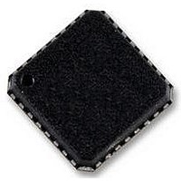
AD9553BCPZ Analog Devices Inc, AD9553BCPZ Datasheet - Page 25

AD9553BCPZ
Manufacturer Part Number
AD9553BCPZ
Description
IC INTEGER-N CLCK GEN 32LFCSP
Manufacturer
Analog Devices Inc
Datasheet
1.AD9553PCBZ.pdf
(44 pages)
Specifications of AD9553BCPZ
Clock Ic Type
PLL Clock Driver
Ic Interface Type
3 Wire, Serial
Frequency
710MHz
No. Of Outputs
2
Supply Current
162mA
Supply Voltage Range
0V To 3.3V
Digital Ic Case Style
LFCSP
Lead Free Status / RoHS Status
Lead free / RoHS Compliant
Available stocks
Company
Part Number
Manufacturer
Quantity
Price
Company:
Part Number:
AD9553BCPZ
Manufacturer:
ADI
Quantity:
154
Output Driver Polarity (CMOS)
When the mode control bits indicate the CMOS logic family
(see Table 19), the user has control of the logic polarity asso-
ciated with each CMOS output pin. Driver polarity defines how
the logic level (Logic 1 or Logic 0) at a CMOS output pin relates
to the logic state (logic true or logic false). Normal polarity
equates Logic 1/Logic 0 to logic true/logic false, while inverted
polarity equates Logic 0/Logic 1 to logic true/logic false. Bit[2]
of the OUT1 and OUT2 driver control registers establishes the
CMOS polarity of the associated output driver (see Figure 31).
Output Drive Strength (CMOS or LVDS)
When the mode bits indicate the CMOS or LVDS logic family
(see Table 19), the user can select whether the output driver
uses weak or strong drive capability. Bit 7 of the OUT1 and
OM[2:0]
3
DEFAULT VALUES
SHOWN IN RED
REGISTER
DECODE
LOGIC
PIN
CONTROL
CONTROL
Figure 31. Output Driver Control
MODE
MODE
3
3
Rev. A | Page 25 of 44
BITS
BITS
[5:3]
[5:3]
MODE
CONTROL
101
101
3
3
3
3
BIT 0
BIT 0
1
0
0
1
STRENGTH
STRENGTH
REGISTER 0x32
ENABLE
SPI
CONTROL
REGISTER 0x34
ENABLE
SPI
CONTROL
0
0
3
OUT2 driver control registers control the drive strength of
the associated output driver (see Figure 31). In the case of the
CMOS family, the strong setting allows for driving increased
capacitive loads. In the case of the LVDS family, the nominal
weak and strong drive currents are 3.5 mA and 7 mA, respectively.
Output Power Down
The AD9553 supports the option of independent power-down
of the output drivers. Bit 6 of the OUT1 and OUT2 driver control
registers controls the power-down function (see Figure 31). When
Bit 6 is Logic 0, the associated output driver is active. When Bit 6 is
Logic 1, the associated output driver is in power-down mode.
DRIVE
DRIVE
BIT 7
BIT 7
1
1
CONTROL
CONTROL
OUTPUT
OUTPUT
DRIVER
DRIVER
BIT 6
BIT 6
POWER-
DOWN
POWER-
DOWN
0
0
BITS
BITS
[2:1]
[2:1]
2
2
CMOS
POLARITY
CMOS
POLARITY
00
00
2
2
OUT1
OUT2
AD9553


