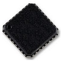
AD9553BCPZ Analog Devices Inc, AD9553BCPZ Datasheet - Page 38

AD9553BCPZ
Manufacturer Part Number
AD9553BCPZ
Description
IC INTEGER-N CLCK GEN 32LFCSP
Manufacturer
Analog Devices Inc
Datasheet
1.AD9553PCBZ.pdf
(44 pages)
Specifications of AD9553BCPZ
Clock Ic Type
PLL Clock Driver
Ic Interface Type
3 Wire, Serial
Frequency
710MHz
No. Of Outputs
2
Supply Current
162mA
Supply Voltage Range
0V To 3.3V
Digital Ic Case Style
LFCSP
Lead Free Status / RoHS Status
Lead free / RoHS Compliant
Available stocks
Company
Part Number
Manufacturer
Quantity
Price
Company:
Part Number:
AD9553BCPZ
Manufacturer:
ADI
Quantity:
154
AD9553
Input Receiver and Band Gap Control (Register 0x1A)
Table 32.
Address
0x1A
XTAL Control (Register 0x1B to Register 0x1E)
Table 33.
Address
0x1B
0x1C
0x1D
0x1E
REFA Frequency Control (Register 0x1F to Register 0x22)
Table 34.
Address
0x1F
0x20
0x21
0x22
Bit
7
6
[5:0]
[7:0]
[7:0]
[7:0]
Bit
7
[6:2]
1
0
Bit
[7:0]
[7:2]
1
0
7
6
5
4
[3:0]
[7:0]
Bit Name
Disable SPI control of XTAL
tuning capacitance
Unused
XTAL tuning capacitor control
Unused
Unused
Unused
Bit Name
Receiver reset
Band gap voltage adjust
Unused
Enable SPI control of band
gap voltage
Bit Name
REFA divider (R
REFA divider (R
Enable SPI control of R
Unused
Enable SPI control of ×2
Select ×2
Enable SPI control of ÷5
Select ÷5
Unused
Unused
A
A
A
A
)
)
A
A
A
Description
Input receiver reset control. This is an autoclearing bit.
0 = normal operation (default).
1 = resets the reference input hardware (detectors, dividers, switchover control,
crystal oscillator, and its associated frequency doubler).
Unused.
Enables functionality of Register 0x1A[6:2].
0 = the device automatically selects receiver band gap voltage (default).
1 = Register 0x1A[6:2] defines the receiver band gap voltage.
Description
Bits[13:6] of the 14-bit REFA divider.
Bits[5:0] of the 14-bit REFA divider (default: R
are ineffective unless Register 0x20[1] = 1.
Enables SPI port control of the REFA divider value (R
0 = the A3 to A0 pins define R
1 = the 14-bit value in the REFA divider register defines R
Unused.
Enables SPI control of the REFA ×2 frequency multiplier (×2
0 = the device automatically selects ×2
1 = Register 0x21[6] controls the selection of ×2
Selects ×2
0 = bypass ×2
1 = select ×2
Enables SPI control of the ÷5
0 = the device automatically selects ÷5
1 = Register 0x21[4] controls the selection of ÷5
Selects ÷5
0 = bypass ÷5
1 = select ÷5
Unused.
Unused.
Controls the band gap voltage setting from minimum (00000) to maximum (11111).
Default is 00000.
The band gap voltage adjust bits are ineffective unless Register 0x1A[0] = 1.
Description
Disables functionality of Register 0x1B[5:0].
0 = tuning capacitance defined by Register 0x1B[5:0].
1 = the device automatically selects XTAL tuning capacitance (default).
When programming this register write a Logic 0 to this bit.
Capacitance value coded as inverted binary (0.25 pF per bit); that is, 111111 is 0 pF,
111110 is 0.25 pF, and so on. The default value, 000000, is 15.75 pF. The XTAL tuning
capacitor bits are ineffective unless Register 0x1B[7] = 0.
Unused.
Unused.
Unused.
Rev. A | Page 38 of 44
A
A
. This bit is ineffective unless Register 0x21[7] = 1.
. This bit is ineffective unless Register 0x21[5] = 1.
A
A
.
.
A
A
(default).
(default)
A
A
prescaler per 0x21[4].
per Table 14 (default).
A
A
per Table 14 (default).
per Table 14 (default).
A
= 4096 decimal). The REFA divider bits
A
A
.
.
A
).
A
.
A
) per 0x21[6].


