ALD7556SBL Advanced Linear Devices Inc, ALD7556SBL Datasheet - Page 3
ALD7556SBL
Manufacturer Part Number
ALD7556SBL
Description
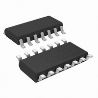
IC TIMER CMOS ANLG RC DL 14SOIC
Manufacturer
Advanced Linear Devices Inc
Type
555 Type, Timer/Oscillator (Dual)r
Datasheet
1.ALD7556SBL.pdf
(12 pages)
Specifications of ALD7556SBL
Package / Case
14-SOIC (0.154", 3.90mm Width)
Current - Supply
100µA
Mounting Type
Surface Mount
Frequency
2.5MHz
Voltage - Supply
2 V ~ 10 V
Operating Temperature
0°C ~ 70°C
Number Of Internal Timers
2
Supply Voltage (max)
10 V
Supply Voltage (min)
2 V
Maximum Power Dissipation
600 mW
Maximum Operating Temperature
+ 70 C
Minimum Operating Temperature
0 C
Mounting Style
SMD/SMT
Lead Free Status / RoHS Status
Lead free / RoHS Compliant
Count
-
Lead Free Status / Rohs Status
Lead free / RoHS Compliant
Other names
1014-1192
Available stocks
Company
Part Number
Manufacturer
Quantity
Price
Company:

Part Number:
ALD7556SBL
Manufacturer:
Linear
Quantity:
259


GENERAL INFORMATION
The ALD7555 and the ALD7556 devices are analog timers
that are, in most situations, direct replacements or direct same
pin-out upgrades for the ICM7555, ICM7556, NE/SE555 and
NE/SE556 devices. Significantly improved performances for
the ALD7555 and the ALD7556 include precision in timing,
reduced leakage currents at all the pin terminals, faster
switching speeds, reduced switching current spikes, en-
hanced discharge output drive currents, better temperature
stability, and better timing stability as a function of power
supply.
These improvements not only improve on the timer function,
but also improve on many of the thousands of circuits that
depend on this timer architecture, such as modulation cir-
cuits, Schmitt triggers, astable circuits, and myriads of mea-
surement and control circuits where the user may have
reached performance limits with their ICM7555, ICM7556,
NE/SE555 and NE/SE556 devices. For a given design, one
or more specification of the timer device may become the
circuit performance limiting factor.
ALD7556 devices are designed to address such limitations
and in many cases offer a solution that is simpler and lower
cost for a given design challenge than by other solutions by
using other circuit means and techniques.
ARCHITECTURE
The ALD7555 and the ALD7556 are analog timers that oper-
ate based on the RC timing principle, using an external tim-
ing resistor R and an external timing capacitor C. The C is
charged by the R and then discharged via one of the two
output pin connections provided by the ALD7555 and the
ALD7556. The control of the two outputs are provided by
one of the 4 input pins. The inputs are named THRESH-
OLD, CONTROL, RESET and TRIGGER. THRESHOLD and
TRIGGER are connected to two separate voltage compara-
tors with their respective comparator control levels set by an
internal resistor string, consisting of three equal-valued and
matched resistors. The output of the two comparators set an
internal RS flip-flop circuit, which in turn controls an OUT-
PUT and a DISCHARGE output. See Block Diagram for a
simplified equivalent circuit. The OUTPUT swings from rail
to rail of the supply voltage, whereas the DISCHARGE only
sinks current when it is active.
The ALD7555 and the ALD7556 operates by charging and
discharging the RC timing between 1/3 and 2/3 V+, and by a
feedback function provided by the user through the OUT-
PUT and/or DISCHAGE pins. This feedback is provided by
the application circuit external connections, which determines
the mode of the circuit operation. The architecture of this
timer takes advantage of the fact that all charging and dis-
charging of C are referenced by the reference resistor string
that provide reference voltages proportional to supply volt-
age V+ (Vdd). As the charging and the discharging of the
capacitor C is also proportional to V+, the frequency of os-
cillation is independent of V+ voltage levels.
ALD7555/ALD7556
The ALD7555 and the
Advanced Linear Devices
APPLICATION NOTES
The three most basic modes of these external connections
are shown as Astable Mode (Free Running Mode), 50% Duty
Cycle Mode, and the Monostable Mode. See Typical Appli-
cations. There are thousands of application circuits devel-
oped that allow the user to manipulate this feedback func-
tion, and which then produces many unique functions that is
beyond a basic timer function. The application versatility of
The ALD7555 and the ALD7556 is only limited by the imagi-
nation of the circuit designer.
LOW POWER SUPPLY REQUIREMENTS
The CMOS process and the design of the ALD7555 and the
ALD7556 devices utilize three well-matched on-chip high
impedance resistors to build the internal reference resistor
string to provide very low power supply operation. Another
technique to achieve low power supply requirement is by
using low power MOSFET circuits on-chip, and by allowing
the user to use a combination of off-chip timing resistor and
capacitor that would reduce their power consumption as well.
Generally, this is accomplished by using higher values for R
and lower values for C in a combination that would still pro-
vide the timing required. Furthermore, reduced on-chip leak-
age currents improve on not only timing precision, but also
greatly increased ranges of usable R and C values to gener-
ate the same RC time constant.
ENHANCED DISCHARGE OUTPUT DRIVE
The Discharge Output Drive Currents of the ALD7555 and
the ALD7556 devices are increased significantly (80mA)
when compared to other timers so that in many applications
where the user may use this output as an output driver in-
stead of having to add another output driver or buffer cir-
cuitry. For example, in many situations, the Discharge Out-
put Drive Current is sufficient to drive a relay or a Power
MOSFET directly.
ASTABLE OPERATION
ALD7555 and the ALD7556 devices are designed to func-
tion as astable oscillators. These timers can be connected
to self trigger and run as a free running mutivibrator. In the
free running oscillator mode, the external capacitor C is
charged through Ra and Rb, and it is discharged through Rb
only. By adjusting the values of Ra and Rb in combination
with the value of C, both the frequency and the duty cycle of
the oscillator pulse can be adjusted. In the 50% astable mode,
the charging and the discharging of C are performed by the
same R between the same voltage levels set by the refer-
ence resistor string, and therefore timer provide a true 50%
duty cycle square wave that is symmetrical. (See typical
applications)
3 of 12
Related parts for ALD7556SBL
Image
Part Number
Description
Manufacturer
Datasheet
Request
R

Part Number:
Description:
MODULE ENERGY HARVESTER W/CONN
Manufacturer:
Advanced Linear Devices Inc
Datasheet:

Part Number:
Description:
MODULE ENERGY HARVESTER W/CONN
Manufacturer:
Advanced Linear Devices Inc
Datasheet:

Part Number:
Description:
MODULE ENERGY HARVESTER W/CONN
Manufacturer:
Advanced Linear Devices Inc
Datasheet:

Part Number:
Description:
MODULE ENERGY HARVESTER W/CONN
Manufacturer:
Advanced Linear Devices Inc
Datasheet:

Part Number:
Description:
IC OPAMP GP R-R CMOS 8SOIC
Manufacturer:
Advanced Linear Devices Inc
Datasheet:
Part Number:
Description:
IC OPAMP GP R-R CMOS 8SOIC
Manufacturer:
Advanced Linear Devices Inc
Datasheet:

Part Number:
Description:
IC OPAMP GP R-R CMOS 8PDIP
Manufacturer:
Advanced Linear Devices Inc
Datasheet:
Part Number:
Description:
IC OPAMP GP R-R CMOS 8PDIP
Manufacturer:
Advanced Linear Devices Inc
Datasheet:
Part Number:
Description:
IC OPAMP GP R-R CMOS 8SOIC
Manufacturer:
Advanced Linear Devices Inc
Datasheet:
Part Number:
Description:
IC OPAMP GP R-R CMOS 8SOIC
Manufacturer:
Advanced Linear Devices Inc
Datasheet:
Part Number:
Description:
IC OPAMP GP R-R CMOS 8PDIP
Manufacturer:
Advanced Linear Devices Inc
Datasheet:
Part Number:
Description:
IC OPAMP GP R-R CMOS 8SOIC
Manufacturer:
Advanced Linear Devices Inc
Datasheet:
Part Number:
Description:
IC OPAMP GP R-R CMOS 8PDIP
Manufacturer:
Advanced Linear Devices Inc
Datasheet:
Part Number:
Description:
IC OPAMP GP R-R CMOS 8PDIP
Manufacturer:
Advanced Linear Devices Inc
Datasheet:
Part Number:
Description:
IC OPAMP GP R-R CMOS 8SOIC
Manufacturer:
Advanced Linear Devices Inc
Datasheet: