ALD7556SBL Advanced Linear Devices Inc, ALD7556SBL Datasheet - Page 4
ALD7556SBL
Manufacturer Part Number
ALD7556SBL
Description
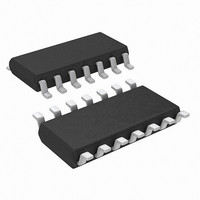
IC TIMER CMOS ANLG RC DL 14SOIC
Manufacturer
Advanced Linear Devices Inc
Type
555 Type, Timer/Oscillator (Dual)r
Datasheet
1.ALD7556SBL.pdf
(12 pages)
Specifications of ALD7556SBL
Package / Case
14-SOIC (0.154", 3.90mm Width)
Current - Supply
100µA
Mounting Type
Surface Mount
Frequency
2.5MHz
Voltage - Supply
2 V ~ 10 V
Operating Temperature
0°C ~ 70°C
Number Of Internal Timers
2
Supply Voltage (max)
10 V
Supply Voltage (min)
2 V
Maximum Power Dissipation
600 mW
Maximum Operating Temperature
+ 70 C
Minimum Operating Temperature
0 C
Mounting Style
SMD/SMT
Lead Free Status / RoHS Status
Lead free / RoHS Compliant
Count
-
Lead Free Status / Rohs Status
Lead free / RoHS Compliant
Other names
1014-1192
Available stocks
Company
Part Number
Manufacturer
Quantity
Price
Company:

Part Number:
ALD7556SBL
Manufacturer:
Linear
Quantity:
259


MONOSTABLE OPERATION
In this mode of operation the ALD7555 and the ALD7556
can be connected as a one-shot circuit which produces an
output pulse with a user-adjustable pulse delay time. The
pulse delay time is set by the external R and C values, which
together produce a RC time constant that is proportional to
the time delay. (See typical applications) The pulse is started
with an external negative going Trigger pulse applied to TRIG-
GER pin. This negative going pulse set an internal flip-flop
so that the external R and C can start the RC timing while
the OUTPUT pin is in the HIGH state. The external C is
being charged by the external R. When the voltage between
the R and C is charged passed the internal threshold volt-
age at the THRESHOLD pin, which is set at 66.6% of V+,
the internal comparator of the ALD7555 and the ALD7556
resets the internal flip-flop. This then turns on the Discharge
Driver at DISCHARGE pin, and discharges the timing ca-
pacitor C. The cycle is completed when the OUTPUT is driven
to a low state and the ALD7555 and the ALD7556 are again
waiting for the next negative going trigger pulse at TRIG-
GER pin.
ALD7555/ALD7556
APPLICATION NOTES (cont’d)
Advanced Linear Devices
CONTROL Voltage and RESET pins
The CONTROL pin directly accesses one input to the upper
comparator. As the input reference resistor string has on-
chip high impedance resistors, an input voltage at the CON-
TROL input can easily change the voltage at the comparator
input. This allows the user to change the oscillation fre-
quency, or modulate the oscillation frequency of the analog
timer, with a separate user provided frequency. The CON-
TROL pin also allows a user-provided inhibit signal to stop
and start the timerís oscillation.
The RESET terminal directly resets the internal RS flip-flop
circuit, which in turn controls the OUTPUT and DISCHARGE
pins. This function is activated by a low voltage input of 0.7V
of 100 ns minimum duration. By injecting a variety of input
signals in a combination to the TRIGGER , THRESHOLD,
CONTROL and RESET pins, many interesting modulation
and demodulation signals can be manipulated and/or gen-
erated by the circuit designer.
4 of 12
Related parts for ALD7556SBL
Image
Part Number
Description
Manufacturer
Datasheet
Request
R

Part Number:
Description:
MODULE ENERGY HARVESTER W/CONN
Manufacturer:
Advanced Linear Devices Inc
Datasheet:

Part Number:
Description:
MODULE ENERGY HARVESTER W/CONN
Manufacturer:
Advanced Linear Devices Inc
Datasheet:

Part Number:
Description:
MODULE ENERGY HARVESTER W/CONN
Manufacturer:
Advanced Linear Devices Inc
Datasheet:

Part Number:
Description:
MODULE ENERGY HARVESTER W/CONN
Manufacturer:
Advanced Linear Devices Inc
Datasheet:

Part Number:
Description:
IC OPAMP GP R-R CMOS 8SOIC
Manufacturer:
Advanced Linear Devices Inc
Datasheet:
Part Number:
Description:
IC OPAMP GP R-R CMOS 8SOIC
Manufacturer:
Advanced Linear Devices Inc
Datasheet:

Part Number:
Description:
IC OPAMP GP R-R CMOS 8PDIP
Manufacturer:
Advanced Linear Devices Inc
Datasheet:
Part Number:
Description:
IC OPAMP GP R-R CMOS 8PDIP
Manufacturer:
Advanced Linear Devices Inc
Datasheet:
Part Number:
Description:
IC OPAMP GP R-R CMOS 8SOIC
Manufacturer:
Advanced Linear Devices Inc
Datasheet:
Part Number:
Description:
IC OPAMP GP R-R CMOS 8SOIC
Manufacturer:
Advanced Linear Devices Inc
Datasheet:
Part Number:
Description:
IC OPAMP GP R-R CMOS 8PDIP
Manufacturer:
Advanced Linear Devices Inc
Datasheet:
Part Number:
Description:
IC OPAMP GP R-R CMOS 8SOIC
Manufacturer:
Advanced Linear Devices Inc
Datasheet:
Part Number:
Description:
IC OPAMP GP R-R CMOS 8PDIP
Manufacturer:
Advanced Linear Devices Inc
Datasheet:
Part Number:
Description:
IC OPAMP GP R-R CMOS 8PDIP
Manufacturer:
Advanced Linear Devices Inc
Datasheet:
Part Number:
Description:
IC OPAMP GP R-R CMOS 8SOIC
Manufacturer:
Advanced Linear Devices Inc
Datasheet: