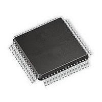
PIC16LF1526-I/MR Microchip Technology, PIC16LF1526-I/MR Datasheet - Page 24

PIC16LF1526-I/MR
Manufacturer Part Number
PIC16LF1526-I/MR
Description
MCU PIC 14KB FLASH 64QFN
Manufacturer
Microchip Technology
Series
PIC® XLP™ 16Fr
Datasheet
1.PIC16LF1526T-IPT.pdf
(354 pages)
Specifications of PIC16LF1526-I/MR
Core Processor
PIC
Core Size
8-Bit
Speed
20MHz
Connectivity
I²C, LIN, SPI, UART/USART
Peripherals
Brown-out Detect/Reset, POR, PWM, WDT
Number Of I /o
54
Program Memory Size
14KB (8K x 14)
Program Memory Type
FLASH
Ram Size
768 x 8
Voltage - Supply (vcc/vdd)
1.8 V ~ 3.6 V
Data Converters
A/D 30x10b
Oscillator Type
Internal
Operating Temperature
-40°C ~ 85°C
Package / Case
64-VFQFN Exposed Pad
Processor Series
PIC16LF
Core
PIC
Data Bus Width
8 bit
Data Ram Size
768 B
Interface Type
SPI, I2C
Maximum Clock Frequency
20 MHz
Number Of Timers
ÿ6 x 8-bit, 3 x 16-bit
Operating Supply Voltage
1.8 V to 5.5 V
Mounting Style
SMD/SMT
Lead Free Status / RoHS Status
Lead free / RoHS Compliant
Eeprom Size
-
Lead Free Status / Rohs Status
Details
- Current page: 24 of 354
- Download datasheet (3Mb)
PIC16(L)F1526/27
3.2.2
The Special Function Registers are registers used by
the application to control the desired operation of
peripheral functions in the device. The Special Function
Registers occupy the 20 bytes after the core registers of
every data memory bank (addresses x0Ch/x8Ch
through x1Fh/x9Fh). The registers associated with the
operation of the peripherals are described in the
appropriate peripheral chapter of this data sheet.
3.2.3
There are up to 80 bytes of GPR in each data memory
bank. The Special Function Registers occupy the 20
bytes after the core registers of every data memory
bank (addresses x0Ch/x8Ch through x1Fh/x9Fh).
3.2.3.1
The general purpose RAM can be accessed in a
non-banked method via the FSRs. This can simplify
access to large memory structures. See
“Linear Data Memory”
3.2.4
There are 16 bytes of common RAM accessible from all
banks.
DS41458A-page 24
SPECIAL FUNCTION REGISTER
GENERAL PURPOSE RAM
COMMON RAM
Linear Access to GPR
for more information.
Section 3.5.2
Preliminary
FIGURE 3-3:
3.2.5
The memory maps for PIC16(L)F1526/27 is shown in
Table
7-bit Bank Offset
3-3.
DEVICE MEMORY MAPS
0Ch
0Bh
1Fh
6Fh
7Fh
00h
20h
70h
Special Function Registers
BANKED MEMORY
PARTITIONING
General Purpose RAM
2011 Microchip Technology Inc.
(20 bytes maximum)
(80 bytes maximum)
Memory Region
Core Registers
Common RAM
(12 bytes)
(16 bytes)
Related parts for PIC16LF1526-I/MR
Image
Part Number
Description
Manufacturer
Datasheet
Request
R

Part Number:
Description:
IC, 8BIT MCU, PIC16LF, 32MHZ, QFN-28
Manufacturer:
Microchip Technology
Datasheet:

Part Number:
Description:
IC, 8BIT MCU, PIC16LF, 32MHZ, QFN-28
Manufacturer:
Microchip Technology
Datasheet:

Part Number:
Description:
IC, 8BIT MCU, PIC16LF, 32MHZ, DIP-18
Manufacturer:
Microchip Technology
Datasheet:

Part Number:
Description:
IC, 8BIT MCU, PIC16LF, 20MHZ, TQFP-44
Manufacturer:
Microchip Technology
Datasheet:

Part Number:
Description:
7 KB Flash, 384 Bytes RAM, 32 MHz Int. Osc, 16 I/0, Enhanced Mid Range Core, Nan
Manufacturer:
Microchip Technology

Part Number:
Description:
14KB Flash, 512B RAM, LCD, 11x10b ADC, EUSART, NanoWatt XLP 28 SOIC .300in T/R
Manufacturer:
Microchip Technology
Datasheet:

Part Number:
Description:
14KB Flash, 512B RAM, LCD, 11x10b ADC, EUSART, NanoWatt XLP 28 SSOP .209in T/R
Manufacturer:
Microchip Technology
Datasheet:

Part Number:
Description:
MCU PIC 14KB FLASH XLP 28-SSOP
Manufacturer:
Microchip Technology

Part Number:
Description:
MCU PIC 14KB FLASH XLP 28-SOIC
Manufacturer:
Microchip Technology

Part Number:
Description:
MCU PIC 512B FLASH XLP 28-UQFN
Manufacturer:
Microchip Technology

Part Number:
Description:
MCU PIC 14KB FLASH XLP 28-SPDIP
Manufacturer:
Microchip Technology

Part Number:
Description:
MCU 7KB FLASH 256B RAM 40-UQFN
Manufacturer:
Microchip Technology

Part Number:
Description:
MCU 7KB FLASH 256B RAM 44-TQFP
Manufacturer:
Microchip Technology

Part Number:
Description:
MCU 14KB FLASH 1KB RAM 28-UQFN
Manufacturer:
Microchip Technology

Part Number:
Description:
MCU PIC 14KB FLASH XLP 40-UQFN
Manufacturer:
Microchip Technology


