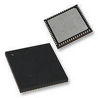
PIC16LF1527-I/MR Microchip Technology, PIC16LF1527-I/MR Datasheet - Page 117

PIC16LF1527-I/MR
Manufacturer Part Number
PIC16LF1527-I/MR
Description
MCU PIC 28KB FLASH 64QFN
Manufacturer
Microchip Technology
Series
PIC® XLP™ 16Fr
Datasheet
1.PIC16LF1526T-IPT.pdf
(354 pages)
Specifications of PIC16LF1527-I/MR
Core Processor
PIC
Core Size
8-Bit
Speed
20MHz
Connectivity
I²C, LIN, SPI, UART/USART
Peripherals
Brown-out Detect/Reset, POR, PWM, WDT
Number Of I /o
54
Program Memory Size
28KB (16K x 14)
Program Memory Type
FLASH
Ram Size
1.5K x 8
Voltage - Supply (vcc/vdd)
1.8 V ~ 3.6 V
Data Converters
A/D 30x10b
Oscillator Type
Internal
Operating Temperature
-40°C ~ 85°C
Package / Case
64-VFQFN Exposed Pad
Processor Series
PIC16F
Core
PIC
Data Ram Size
768 B
Interface Type
MI2C, SPI, EUSART
Number Of Timers
9
Operating Supply Voltage
1.8 V to 5.5 V
Maximum Operating Temperature
+ 85 C
Mounting Style
SMD/SMT
Development Tools By Supplier
MPLAB IDE Software
Minimum Operating Temperature
- 40 C
Lead Free Status / RoHS Status
Lead free / RoHS Compliant
Eeprom Size
-
Lead Free Status / Rohs Status
Details
- Current page: 117 of 354
- Download datasheet (3Mb)
12.0
In general, when a peripheral is enabled on a port pin,
that pin cannot be used as a general purpose output.
However, the pin can still be read.
Each port has three standard registers for its operation.
These registers are:
• TRISx registers (data direction)
• PORTx registers (reads the levels on the pins of
• LATx registers (output latch)
Some ports may have one or more of the following
additional registers. These registers are:
• ANSELx (analog select)
• WPUx (weak pull-up)
TABLE 12-1:
The Data Latch (LATA register) is useful for
read-modify-write operations on the value that the I/O
pins are driving.
A write operation to the LATA register has the same
affect as a write to the corresponding PORTA register.
A read of the LATA register reads of the values held in
the I/O PORT latches, while a read of the PORTA
register reads the actual I/O pin value.
The port has analog functions and has an ANSELA
register which can disable the digital input and save
power. A simplified model of a generic I/O port, without
the interfaces to other peripherals, is shown in
Figure
2011 Microchip Technology Inc.
Device
PIC16(L)F1526
PIC16(L)F1527
the device)
12-1.
I/O PORTS
PORT AVAILABILITY PER
DEVICE
●
●
●
●
●
●
●
●
●
●
●
●
Preliminary
●
●
FIGURE 12-1:
EXAMPLE 12-1:
; This code example illustrates
; initializing the PORTA register. The
; other ports are initialized in the same
; manner.
BANKSEL PORTA
CLRF
BANKSEL LATA
CLRF
BANKSEL ANSELA
CLRF
BANKSEL TRISA
MOVLW
MOVWF
To peripherals
Write PORTx
Write LATx
Data Bus
Read PORTx
PIC16(L)F1526/27
PORTA
LATA
ANSELA
B'00111000' ;Set RA<5:3> as inputs
TRISA
Data Register
D
CK
Read LATx
ANSELx
GENERIC I/O PORT
OPERATION
INITIALIZING PORTA
Q
;
;Init PORTA
;Data Latch
;
;
;digital I/O
;
;and set RA<2:0> as
;outputs
TRISx
DS41458A-page 117
V
V
DD
SS
I/O pin
Related parts for PIC16LF1527-I/MR
Image
Part Number
Description
Manufacturer
Datasheet
Request
R

Part Number:
Description:
IC, 8BIT MCU, PIC16LF, 32MHZ, QFN-28
Manufacturer:
Microchip Technology
Datasheet:

Part Number:
Description:
IC, 8BIT MCU, PIC16LF, 32MHZ, QFN-28
Manufacturer:
Microchip Technology
Datasheet:

Part Number:
Description:
IC, 8BIT MCU, PIC16LF, 32MHZ, DIP-18
Manufacturer:
Microchip Technology
Datasheet:

Part Number:
Description:
IC, 8BIT MCU, PIC16LF, 20MHZ, TQFP-44
Manufacturer:
Microchip Technology
Datasheet:

Part Number:
Description:
7 KB Flash, 384 Bytes RAM, 32 MHz Int. Osc, 16 I/0, Enhanced Mid Range Core, Nan
Manufacturer:
Microchip Technology

Part Number:
Description:
14KB Flash, 512B RAM, LCD, 11x10b ADC, EUSART, NanoWatt XLP 28 SOIC .300in T/R
Manufacturer:
Microchip Technology
Datasheet:

Part Number:
Description:
14KB Flash, 512B RAM, LCD, 11x10b ADC, EUSART, NanoWatt XLP 28 SSOP .209in T/R
Manufacturer:
Microchip Technology
Datasheet:

Part Number:
Description:
MCU PIC 14KB FLASH XLP 28-SSOP
Manufacturer:
Microchip Technology

Part Number:
Description:
MCU PIC 14KB FLASH XLP 28-SOIC
Manufacturer:
Microchip Technology

Part Number:
Description:
MCU PIC 512B FLASH XLP 28-UQFN
Manufacturer:
Microchip Technology

Part Number:
Description:
MCU PIC 14KB FLASH XLP 28-SPDIP
Manufacturer:
Microchip Technology

Part Number:
Description:
MCU 7KB FLASH 256B RAM 40-UQFN
Manufacturer:
Microchip Technology

Part Number:
Description:
MCU 7KB FLASH 256B RAM 44-TQFP
Manufacturer:
Microchip Technology

Part Number:
Description:
MCU 14KB FLASH 1KB RAM 28-UQFN
Manufacturer:
Microchip Technology

Part Number:
Description:
MCU PIC 14KB FLASH XLP 40-UQFN
Manufacturer:
Microchip Technology


