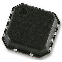
ADV3220ACPZ Analog Devices Inc, ADV3220ACPZ Datasheet - Page 17

ADV3220ACPZ
Manufacturer Part Number
ADV3220ACPZ
Description
IC MULTIPLEXER 2:1 16LFCSP
Manufacturer
Analog Devices Inc
Datasheet
1.ADV3219ACPZ.pdf
(20 pages)
Specifications of ADV3220ACPZ
Supply Voltage Range
± 4.5V To ± 5.5V
Supply Current
7.5mA
Digital Ic Case Style
LFCSP
No. Of Pins
8
Operating Temperature Range
-40°C To +85°C
Svhc
No SVHC (18-Jun-2010)
Base Number
322
Lead Free Status / RoHS Status
Lead free / RoHS Compliant
ADV3219/ADV3220
APPLICATIONS INFORMATION
The ADV3219 and ADV3220 are very high speed muxes that
can be used to switch video or RF signals. The low output imped-
ance of the ADV3219/ADV3220 allows the output environment
to be optimized for use in 75 Ω or 50 Ω systems by choosing the
appropriate series termination resistor. For composite video
applications, the ADV3220 (gain of +2) is typically used to
provide compensation for the loss of the output termination.
CIRCUIT LAYOUT
Use of proper high speed design techniques is important to
ensure optimum performance. Use a low inductance ground
plane for power supply bypassing and to provide high quality
return paths for the input and output signals. For best performance,
it is recommended that power supplies be bypassed with 0.1 μF
ceramic capacitors placed as close to the body of the device as
possible. To provide stored energy for lower frequency, high
current output driving, place 10 μF tantalum capacitors farther
from the device.
The input and output signal paths should be stripline or micro-
strip controlled impedance. Video systems typically use a 75 Ω
characteristic impedance, whereas RF systems typically use 50 Ω.
Various calculators are available to calculate the trace geometry
that is required to produce the proper characteristic impedance.
Rev. 0 | Page 17 of 20
TERMINATION
For a controlled impedance situation, termination resistors are
required at the inputs and output of the device. The input ter-
mination should be a shunt resistor to ground with a value
matching the characteristic impedance of the input trace. To
reduce reflections, place the input termination resistor as close
to the device input pin as possible. To minimize the input-to-
input crosstalk, it is important to use a low inductance shield
between input traces to isolate each input. Consideration of
ground current paths must be taken to minimize loop currents
in the shields to prevent them from providing a coupling medium
for crosstalk.
For proper matching, the output series termination resistor
should be the same value as the characteristic impedance of the
output trace and placed as close to the output of the device as
possible. This placement reduces the high frequency effect of
series parasitic inductance, which can affect gain flatness and
−3 dB bandwidth.
CAPACITIVE LOAD
A high frequency output generally has difficulty when driving a
capacitive load. The usual response is some peaking in the fre-
quency domain or some overshoot in the time domain. If these
effects become too large, oscillation can result.
The response of the device under various capacitive loads is
shown in Figure 4 to Figure 10 and in Figure 13. If a condition
arises wherein excessive load capacitance is encountered and
the overshoot is too great or the part oscillates, use a small series
resistor of a few tens of ohms to improve the performance.


