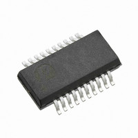
PI74FCT245TQEX Pericom Semiconductor, PI74FCT245TQEX Datasheet - Page 2

PI74FCT245TQEX
Manufacturer Part Number
PI74FCT245TQEX
Description
IC TXRX OCTAL BIDIR 20QSOP
Manufacturer
Pericom Semiconductor
Datasheet
1.PI74FCT245ATQ.pdf
(7 pages)
Specifications of PI74FCT245TQEX
Lead Free Status / RoHS Status
Lead free / RoHS Compliant
1 2 3 4 5 6 7 8 9 0 1 2 3 4 5 6 7 8 9 0 1 2 3 4 5 6 7 8 9 0 1 2 1 2 3 4 5 6 7 8 9 0 1 2 3 4 5 6 7 8 9 0 1 2 3 4 5 6 7 8 9 0 1 2 1 2 3 4 5 6 7 8 9 0 1 2 3 4 5 6 7 8 9 0 1 2 3 4 5 6 7 8 9 0 1 2 1 2 3 4 5 6 7 8 9 0 1 2 3 4 5 6 7 8 9 0 1 2 3 4 5 6 7 8 9 0 1 2 1 2 3 4 5 6 7 8 9 0 1 2
1 2 3 4 5 6 7 8 9 0 1 2 3 4 5 6 7 8 9 0 1 2 3 4 5 6 7 8 9 0 1 2 1 2 3 4 5 6 7 8 9 0 1 2 3 4 5 6 7 8 9 0 1 2 3 4 5 6 7 8 9 0 1 2 1 2 3 4 5 6 7 8 9 0 1 2 3 4 5 6 7 8 9 0 1 2 3 4 5 6 7 8 9 0 1 2 1 2 3 4 5 6 7 8 9 0 1 2 3 4 5 6 7 8 9 0 1 2 3 4 5 6 7 8 9 0 1 2 1 2 3 4 5 6 7 8 9 0 1 2
Maximum Ratings
(Above which the useful life may be impaired. For user guidelines, not tested.)
Notes:
1. For Max. or Min. conditions, use appropriate value specified under Electrical Characteristics for the applicable device type.
2. Typical values are at V
3. Not more than one output should be shorted at one time. Duration of the test should not exceed one second.
Capacitance
Notes:
1. These Parameters are determined by device characterization but are not production tested.
DC Electrical Characteristics
Parameters
Parameters Description
Storage Temperature .................................................................... –65°C to +150°C
Ambient Temperature with Power Applied .................................... –40°C to +85°C
Supply Voltage to Ground Potential (Inputs & V
Supply Voltage to Ground Potential (Outputs & D/O Only) ........... –0.5V to +7.0V
DC Input Voltage ............................................................................ –0.5V to +7.0V
DC Output Current ...................................................................................... 120mA
Power Dissipation ..........................................................................................0.5W
V
V
V
V
V
I
I
I
I
I
I
V
I
I
V
OS
IH
IL
IH
IL
OZH
OZL
OFF
C
C
H
OH
OL
OL
IH
IL
IK
IN
OUT
06-0207
(1)
Output HIGH Voltage
Output LOW Current
Output LOW Current
Input HIGH Voltage
Input LOW Voltage
Input HIGH Current
Input LOW Current
Input HIGH Current
Input LOW Current
High Impedance
Output Current
Clamp Diode Voltage
Power Down Disable
Short Circuit Current
Input Hysteresis
(T
A
= 25°C, f = 1 MHz)
Description
Input Capacitance
Output Capacitance
CC
= 5.0V, +25°C ambient and maximum loading.
(Over the Operating Range, T
Test Conditions
V
V
V
Guaranteed Logic HIGH Level
Guaranteed Logic LOW Level
(Except I/O pins) V
(I/O pins Only) V
V
V
V
V
(Except I/O pins) V
(I/O pins Only) V
CC
CC
CC
CC
CC
CC
CC
= GND, V
= Min., V
= Min., V
= Min., V
= M
= Min., I
= Max.
AX
CC
Test Conditions
V
V
.
(3)
Only) ............. –0.5V to +7.0V
IN
OUT
IN
, V
IN
IN
IN
OUT
= 0V
= –18 mA
(1)
= V
= V
= V
OUT
CC
CC
= 0V
= 4.5V
CC
CC
= Max.
= Max.
IH
IH
IH
= GND
= Max.
= Max.
or V
or V
or V
2
IL
IL
IL
A
= –40°C to +85°C, V
I
I
I
V
V
V
V
V
V
OH
OL
OL
IN
IN
IN
IN
OUT
OUT
= 64mA
= 12mA (25Ω Series)
= –15.0mA
= GND
= GND
= V
= V
= 2.7V
= 0.5V
CC
CC
Note:
Stresses greater than those listed under MAXIMUM
RATINGS may cause permanent damage to the device.
This is a stress rating only and functional operation
of the device at these or any other conditions above
those indicated in the operational sections of this
specification is not implied. Exposure to absolute
maximum rating conditions for extended periods may
affect reliability.
CC
Typ.
PI74FCT2245T(25 Ohm Series )
Octal BidirectionalTransceivers
= 5.0V ±5%)
6
8
Min. Typ
–60
2.4
2.0
Max.
10
12
–120
–0.7
200
3.0
0.3
0.3
(2)
PI74FCT245T
PS2012E
Units
Max. Units
0.55
0.50
–1.2
100
pF
pF
0.8
–1
–1
–1
1
1
1
mA
μA
μA
μA
μA
μA
μA
μA
m V
08/08/06
V
V
V
V
V
V


