24LC256-E/MF Microchip Technology, 24LC256-E/MF Datasheet - Page 6
24LC256-E/MF
Manufacturer Part Number
24LC256-E/MF
Description
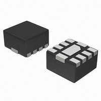
IC EEPROM 256KBIT 400KHZ 8DFN
Manufacturer
Microchip Technology
Datasheet
1.24AA256-ISM.pdf
(34 pages)
Specifications of 24LC256-E/MF
Format - Memory
EEPROMs - Serial
Memory Type
EEPROM
Memory Size
256K (32K x 8)
Speed
400kHz
Interface
I²C, 2-Wire Serial
Voltage - Supply
2.5 V ~ 5.5 V
Operating Temperature
-40°C ~ 125°C
Package / Case
8-VDFN Exposed Pad
Lead Free Status / RoHS Status
Lead free / RoHS Compliant


24AA256/24LC256/24FC256
4.0
The following bus protocol has been defined:
• Data transfer may be initiated only when the bus
• During data transfer, the data line must remain
Accordingly, the following bus conditions have been
defined (Figure 4-1).
4.1
Both data and clock lines remain high.
4.2
A high-to-low transition of the SDA line while the clock
(SCL) is high, determines a Start condition. All
commands must be preceded by a Start condition.
4.3
A low-to-high transition of the SDA line, while the clock
(SCL) is high, determines a Stop condition. All
operations must end with a Stop condition.
DS21203Q-page 6
is not busy.
stable whenever the clock line is high. Changes in
the data line, while the clock line is high, will be
interpreted as a Start or Stop condition.
BUS CHARACTERISTICS
Bus Not Busy (A)
Start Data Transfer (B)
Stop Data Transfer (C)
4.4
The state of the data line represents valid data when,
after a Start condition, the data line is stable for the
duration of the high period of the clock signal.
The data on the line must be changed during the low
period of the clock signal. There is one bit of data per
clock pulse.
Each data transfer is initiated with a Start condition and
terminated with a Stop condition. The number of the
data bytes transferred between the Start and Stop
conditions is determined by the master device.
4.5
Each receiving device, when addressed, is obliged to
generate an Acknowledge signal after the reception of
each byte. The master device must generate an extra
clock pulse which is associated with this Acknowledge
bit.
A device that acknowledges must pull down the SDA
line during the acknowledge clock pulse in such a way
that the SDA line is stable low during the high period of
the acknowledge related clock pulse. Of course, setup
and hold times must be taken into account. During
reads, a master must signal an end of data to the slave
by NOT generating an Acknowledge bit on the last byte
that has been clocked out of the slave. In this case, the
slave (24XX256) will leave the data line high to enable
the master to generate the Stop condition.
Note:
Data Valid (D)
Acknowledge
The 24XX256 does not generate any
Acknowledge
programming cycle is in progress.
2010 Microchip Technology Inc.
bits
if
an
internal
Related parts for 24LC256-E/MF
Image
Part Number
Description
Manufacturer
Datasheet
Request
R

Part Number:
Description:
DICE 0/256K, 32K X 8, 2.5V SER EE DIE IN WAFFLE PK
Manufacturer:
Microchip Technology Inc.
Datasheet:
Part Number:
Description:
SOP8
Manufacturer:
Microchip Technology Inc.
Datasheet:

Part Number:
Description:
IC EEPROM 256KBIT 400KHZ 8SOIC
Manufacturer:
Microchip Technology
Datasheet:

Part Number:
Description:
IC EEPROM 256KBIT 400KHZ 8MSOP
Manufacturer:
Microchip Technology
Datasheet:
Part Number:
Description:
IC EEPROM 256KBIT 400KHZ 8DIP
Manufacturer:
Microchip Technology
Datasheet:

Part Number:
Description:
IC EEPROM 256KBIT 400KHZ 8TSSOP
Manufacturer:
Microchip Technology
Datasheet:
Part Number:
Description:
IC EEPROM 256KBIT 400KHZ 8SOIC
Manufacturer:
Microchip Technology
Datasheet:
Part Number:
Description:
IC EEPROM 256KBIT 400KHZ 8SOIC
Manufacturer:
Microchip Technology
Datasheet:
Part Number:
Description:
IC EEPROM 256KBIT 400KHZ 8SOIC
Manufacturer:
Microchip Technology
Datasheet:
Part Number:
Description:
IC, EEPROM, 256KBIT, I2C, 400KHZ, SOIJ-8
Manufacturer:
Microchip Technology
Datasheet:
Part Number:
Description:
IC EEPROM 256KBIT 400KHZ 8DFN
Manufacturer:
Microchip Technology
Datasheet:
Part Number:
Description:
IC EEPROM 256KBIT 400KHZ 8DIP
Manufacturer:
Microchip Technology
Datasheet:
Part Number:
Description:
IC EEPROM 256KBIT 400KHZ 8SOIC
Manufacturer:
Microchip Technology
Datasheet:
Part Number:
Description:
IC EEPROM 256KBIT 400KHZ 8MSOP
Manufacturer:
Microchip Technology
Datasheet:
Part Number:
Description:
IC EEPROM 256KBIT 400KHZ 8TSSOP
Manufacturer:
Microchip Technology
Datasheet: