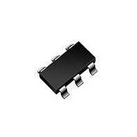
NCP1250ASN65T1G ON Semiconductor, NCP1250ASN65T1G Datasheet - Page 18

NCP1250ASN65T1G
Manufacturer Part Number
NCP1250ASN65T1G
Description
IC PWM CTLR OCP LATCH 6-TSOP
Manufacturer
ON Semiconductor
Datasheet
1.NCP1250ASN65T1G.pdf
(21 pages)
Specifications of NCP1250ASN65T1G
Output Isolation
Isolated
Frequency Range
61kHz ~ 71kHz
Voltage - Input
9.4 V ~ 28 V
Voltage - Output
12V
Operating Temperature
-40°C ~ 125°C
Package / Case
6-TSOP (0.063", 1.60mm Width)
Number Of Outputs
1
Duty Cycle (max)
84 %
Output Current
300 mA
Mounting Style
SMD/SMT
Switching Frequency
65 KHz
Operating Supply Voltage
28 V
Supply Current
2.1 mA
Maximum Operating Temperature
+ 125 C
Fall Time
30 ns
Minimum Operating Temperature
- 40 C
Rise Time
40 ns
Lead Free Status / RoHS Status
Lead free / RoHS Compliant
Available stocks
Company
Part Number
Manufacturer
Quantity
Price
Company:
Part Number:
NCP1250ASN65T1G
Manufacturer:
ON Semiconductor
Quantity:
1 250
Part Number:
NCP1250ASN65T1G
Manufacturer:
ON/安森美
Quantity:
20 000
Then, suppose we want to latch off our controller when V
exceeds 25 V. On the auxiliary winding, the plateau reflects
the output voltage by the turns ratio between the power and
the auxiliary winding. In case of voltage runaway for our
19 V adapter, the plateau will go up to:
1 kW selected OPP pulldown resistor, it implies a 3 mA
current. From 3 V to go up to 18 V, we need an additional
15 V. Under 3 mA and neglecting the series diode forward
drop, it requires a series resistor of:
selected a 15 V Zener diode. In nominal conditions, the
voltage on the OPP pin is almost 0 V during the off time as
the Zener is fully blocked. This technique clearly improves
the noise immunity of the system compared to that obtained
First, calculate the OPP network with the above equations.
Since our OVP comparator trips at a 3 V level, across the
For this configuration to maintain an 18 V level, we have
Figure 46. A Simple Resistive Divider Brings the OPP Pin Above 3 V in Case of a V
100p
22pF
C1
C1
Figure 47. A Zener Diode in Series with a Diode Helps to Improve the Noise Immunity of the System
V
ROPPL
1k
aux,OVP
ROPPL
1k
10
10
+ 25
OPP
OP P
Vlatch
Vlatch
0.18
0.25
5
4
+ 18 V
4
5
D3
15V
R3
5k
ROPPU
421k
RoppU
421k
11
(eq. 15)
http://onsemi.com
1
1
OVP
out
OVP
18 V
11
18
D2
1N4148
D2
1N4148
14 V. Given the divide−by−6 ratio, the OPP pin will swing
to 14/6 = 2.3 V during normal conditions, leaving 700 mV
margin. A 100 pF capacitor can be added between the OPP
pin and GND to improve noise immunity and avoid erratic
trips in presence of external surges. Do not increase this
capacitor too much otherwise the OPP signal will be affected
by the integrating time constant.
a Zener diode wired as recommended by.
from a resistive string as in Figure 46. Please note the
reduction of the capacitor on the OPP pin to 10 pF − 22 pF.
This capacitor is necessary because of the potential spike
coupling through the Zener parasitic capacitance from the
bias winding due to the leakage inductance. Despite the 1 ms
R
In nominal conditions, the plateau establishes to around
A second solution for the OVP detection alone, is to use
OVP
+
V
V
latch
OVP
OPP
OPP
* V
R
OPPL
VOP
+
CC
VCC
VCC
18 * 3
3 1k
Voltage Runaway above
+
9
9
3m
15
+ 5 kW
8
8
aux.
winding
aux.
winding
(eq. 16)


