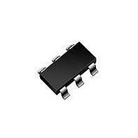
NCP1250ASN65T1G ON Semiconductor, NCP1250ASN65T1G Datasheet - Page 19

NCP1250ASN65T1G
Manufacturer Part Number
NCP1250ASN65T1G
Description
IC PWM CTLR OCP LATCH 6-TSOP
Manufacturer
ON Semiconductor
Datasheet
1.NCP1250ASN65T1G.pdf
(21 pages)
Specifications of NCP1250ASN65T1G
Output Isolation
Isolated
Frequency Range
61kHz ~ 71kHz
Voltage - Input
9.4 V ~ 28 V
Voltage - Output
12V
Operating Temperature
-40°C ~ 125°C
Package / Case
6-TSOP (0.063", 1.60mm Width)
Number Of Outputs
1
Duty Cycle (max)
84 %
Output Current
300 mA
Mounting Style
SMD/SMT
Switching Frequency
65 KHz
Operating Supply Voltage
28 V
Supply Current
2.1 mA
Maximum Operating Temperature
+ 125 C
Fall Time
30 ns
Minimum Operating Temperature
- 40 C
Rise Time
40 ns
Lead Free Status / RoHS Status
Lead free / RoHS Compliant
Available stocks
Company
Part Number
Manufacturer
Quantity
Price
Company:
Part Number:
NCP1250ASN65T1G
Manufacturer:
ON Semiconductor
Quantity:
1 250
Part Number:
NCP1250ASN65T1G
Manufacturer:
ON/安森美
Quantity:
20 000
blanking delay at turn off. This spike is energetic enough to
charge the added capacitor C
could make it discharge slower, potentially disturbing the
blanking circuit. When implementing the Zener option, it is
important to carefully observe the OPP pin voltage (short
probe connections!) and check that enough margin exists to
that respect.
Over Temperature Protection
thermal runaways, e.g. when the temperature inside the
voltage on the auxiliary diode was 13 V in nominal
conditions. We have selected an NTC which offers a
resistance of 470 kW at 25°C and drops to 8.8 kW at 110°C.
If our auxiliary winding plateau is 14 V and we consider a
0.6 V forward drop for the diode, then the voltage across the
NTC in fault mode must be:
through the device must be:
calculated:
calculate the upper resistor value R
Figure 48. The Internal Circuitry Hooked to Pin 3 Can Be Used to Implement Over Temperature Protection (OTP)
In a lot of designs, the adapter must be protected against
Back to our 19 V adapter, we have found that the plateau
Based on the 8.8 kW NTC resistor at 110 °C, the current
As such, the bottom resistor R
Now that the pulldown OPP resistor is known, we can
ROPPL
2.5k
V
NTC
R
OP P
OPPL
I
NTC
+ 14 * 3 * 0.6 + 10.4 V
Vlatch
+
+
10.4
8.8k
1.2m
3
NT C
1
and given the time constant,
[ 1.2 mA
+ 2.5 kW
ROPPU
OPPU
841k
OPPL
1N4148
D2
to adjust the power
, can easily be
full−latch
(eq. 17)
(eq. 18)
(eq. 19)
http://onsemi.com
19
adapter box increases above a certain value. Figure 48
shows how to implement a simple OTP using an external
NTC and a series diode. The principle remains the same:
make sure the OPP network is not affected by the additional
NTC hence the presence of this isolation diode. When the
NTC resistance decreases as the temperature increases, the
voltage on the OPP pin during the off time will slowly
increase and, once it passes 3 V for 4 consecutive clock
cycles, the controller will permanently latch off.
limit at the chosen output power level. Suppose we need a
200 mV decrease from the 0.8 V set point and the on−time
swing on the auxiliary anode is −67.5 V, then we need to drop
over R
The current flowing in the pulldown resistor R
condition will be:
The R
Combining OVP and OTP
together as illustrated by Figure 49.
The OTP and Zener−based OVP can be combined
OPPU
OPPU
OPP
value is therefore easily derived:
a voltage of:
V
ROPPU
I
R
ROPPU
OPPU
+ 67.5 * 0.2 + 67.3 V
+
+
VCC
67.3
200m
80m
2.5k
+ 841 kW
+ 80 mA
OPPL
au x.
winding
(eq. 20)
(eq. 21)
(eq. 22)
in this


