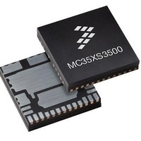
MC35XS3500PNA Freescale Semiconductor, MC35XS3500PNA Datasheet - Page 26

MC35XS3500PNA
Manufacturer Part Number
MC35XS3500PNA
Description
IC SWITCH HIGHSIDE 24PQFN
Manufacturer
Freescale Semiconductor
Type
High Side Switchr
Datasheet
1.MC35XS3500PNAR2.pdf
(41 pages)
Specifications of MC35XS3500PNA
Number Of Outputs
5
Rds (on)
*
Internal Switch(s)
Yes
Current Limit
9A
Voltage - Input
7 V ~ 20 V
Operating Temperature
-40°C ~ 125°C
Mounting Type
Surface Mount
Package / Case
24-PQFN, 24-PowerQFN
Product
MOSFET Gate Drivers
Rise Time
50 ns
Fall Time
50 ns
Propagation Delay Time
6.5 ms
Supply Voltage (max)
+ 5.5 V
Supply Voltage (min)
- 0.3 V
Supply Current
20 mA
Maximum Operating Temperature
+ 125
Minimum Operating Temperature
- 40 C
Lead Free Status / RoHS Status
Lead free / RoHS Compliant
Available stocks
Company
Part Number
Manufacturer
Quantity
Price
between different corner light devices. The register bits D1
and D0 determine the content of the 16 bits of SO data.
(Refer to the section entitled
(Device Status Return Data)
D9 : D2 are described in
ADDRESS 00001 — Configuration OL
load detection for LEDs in Normal mode (OLLEDn in
page 25) and to active the LED Control.
circuit for LED is activated for output 1. When bit D0 is set to
logic [0], open load detection circuit for standard bulbs is
activated for output 1.
for output 1.
ADDRESS 00010 — CONFIGURATION PRESCALER
AND SR
The Configuration Prescaler when D9 bit is set to logic [0] and
Configuration SR when D9 bit is set to logic [1].
PWM clock prescaler per output. When the corresponding
PR bit is set to logic [1], the clock prescaler (reference clock
divided by 2) is activated for the dedicated output.
slew-rate by a factor of 2. When the corresponding SR bit is
set to logic [1], the output switching time is divided by 2 for the
dedicated output.
ADDRESS 00011 — CONFIGURATION CSNS
disable the high over-current shutdown phase (OCHI1 and
26
35XS350
FUNCTIONAL DEVICE OPERATION
LOGIC COMMANDS AND REGISTERS
x = Don’t care
D6 (PWM sync) = 0, No synchronization
D6 (PWM sync) = 1, Synchronization on CSB positive edge
D7 (STOPen) = 0, STOP pin does not control the output 4.
D7 (STOPen) = 1, STOP pin controls the output 4.
D15
The Configuration OL register is used to enable the open
When bit D0 is set to logic [1], the open load detection
When bit D5 is set to logic [1], the LED Control is activated
Two configuration registers are available at this address.
The Configuration Prescaler register is used to enable the
The SR Prescaler register is used to increase the output
The Configuration Current Sense register is used to
0
D14
0
SI Address
D13
0
Table
D12
0
Serial Output Communication
beginning on page 27.) Bits
9.
D11
0
D10
WD
Table 9. Initialization Register
D9
0
Table
D8
0
8,
STOPen
D4, D3, D2 (MUX2, MUX1, MUX0) = 000, No current sense
D4, D3, D2 (MUX2, MUX1, MUX0) = 001, OUT1 current sense
D4, D3, D2 (MUX2, MUX1, MUX0) = 010,current sense
D4, D3, D2 (MUX2, MUX1, MUX0) = 011, OUT3 current sense
D4, D3, D2 (MUX2, MUX1, MUX0) = 100, OUT4 current sense
D4, D3, D2 (MUX2, MUX1, MUX0) = 101, OUT5 current sense
D4, D3, D2 (MUX2, MUX1, MUX0) = 110, External Switch current sense
D4, D3, D2 (MUX2, MUX1, MUX0) = 111, Temperature analog feedback
D7
parameter. As long as the WD bit (D10) of an incoming SPI
message is toggled within the minimum watchdog timeout
period (WDTO), the device will operate normally. If an
internal watchdog timeout occurs before the WD bit is
toggled, the device will revert to Fail mode. All registers are
cleared. To exit the Fail mode, send valid SPI communication
with WD bit = 1.
OCHI2 dynamic levels) in order to activate immediately the
current sense analog feedback.
synchronization signal is reported on FETOUT output pin.
the output is only protected with OCLO level. And the current
sense is immediately available if it is selected through SPI, as
described in
automatically reset at each corresponding ONoff bit transition
from logic [1] to [0] and in case of over-temperature or over-
current fault. All NO_OCHI bits are also reset in case of
under-voltage fault detection.
ADDRESS 01001 — Control OUT1
Table
with bit D7 at logic [0]. This register allows the master to
control the duty cycle and the switching phases of OUT1. The
duty cycle resolution is given by bits D6 : D0.
The watchdog timeout is specified by the
When bit D9 is set to logic [1], the current sense
When the corresponding NO_OCHI bit is set to logic [1],
Bits D9 and D8 control the switching phases as shown in
Bit D7 at logic [1] turns ON OUT1. OUT1 is turned OFF
D7 = 0, D6 : D0 = XX output OFF.
10.
PWM
sync
D6
SI Data
Figures
D9 : D8
Table 10. Switching Phases
D5
0
00
01
10
11
13. The NO_OCHI bit per output is
MUX2
Analog Integrated Circuit Device Data
D4
MUX1
D3
Freescale Semiconductor
PWM Phase
MUX0
D2
180°
270°
90°
0°
t
WDTO
SOA1
D1
SOA0
D0


