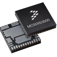
MC35XS3500PNA Freescale Semiconductor, MC35XS3500PNA Datasheet - Page 6

MC35XS3500PNA
Manufacturer Part Number
MC35XS3500PNA
Description
IC SWITCH HIGHSIDE 24PQFN
Manufacturer
Freescale Semiconductor
Type
High Side Switchr
Datasheet
1.MC35XS3500PNAR2.pdf
(41 pages)
Specifications of MC35XS3500PNA
Number Of Outputs
5
Rds (on)
*
Internal Switch(s)
Yes
Current Limit
9A
Voltage - Input
7 V ~ 20 V
Operating Temperature
-40°C ~ 125°C
Mounting Type
Surface Mount
Package / Case
24-PQFN, 24-PowerQFN
Product
MOSFET Gate Drivers
Rise Time
50 ns
Fall Time
50 ns
Propagation Delay Time
6.5 ms
Supply Voltage (max)
+ 5.5 V
Supply Voltage (min)
- 0.3 V
Supply Current
20 mA
Maximum Operating Temperature
+ 125
Minimum Operating Temperature
- 40 C
Lead Free Status / RoHS Status
Lead free / RoHS Compliant
Available stocks
Company
Part Number
Manufacturer
Quantity
Price
Table 3. Static Electrical Characteristics
Characteristics noted under conditions 3.0V ≤ V
Typical values noted reflect the approximate parameter mean at T
POWER INPUT (VBAT, VCC)
LOGIC INPUT/ OUTPUT (IGN, CS, CSNS, SI, SCLK, CLOCK, SO, FLASHER, RST, LIMP, STOP)
Notes
6
35XS350
ELECTRICAL CHARACTERISTICS
STATIC ELECTRICAL CHARACTERISTICS
Battery Supply Voltage Range
Battery Supply Under-voltage (UV flag is set ON)
Battery Voltage Clamp (OV flag is set ON)
Battery Voltage Clamp
Battery Supply Power on Reset
VBAT Supply Current @ 25
Digital Voltage Range, Full Performance
Digital Supply Under-voltage (VCC Failure)
Sleep Current Consumption on V
Supply Current Consumption on V
Input High Logic Level
Input Low Logic Level
Ignition Threshold Level (IGN, FLASHER, STOP and RST)
Input Clamp Voltage (IGN, FLASHER, LIMP, STOP, CS, SCLK, SI, RST)
Input Forward Voltage (IGN, FLASHER, LIMP, STOP, CS, SCLK, SI, RST)
Input Passive Pull-up Resistance on
Input Passive Pull-down Resistance on SI, SCLK, FLASHER, IGN, FOG,
CLOCK, LIMP and RST pins
SO High-state Output Voltage
5.
6.
7.
8.
Full Performance and Short Circuit
Extended Voltage Range
Sleep State Current, Outputs Open
Sleep State Current, Outputs Grounded
Normal Mode, IGN = 5.0 V, RST = 5.0 V, Outputs Open
Output OFF
No SPI
3.0 MHz SPI Communication
I = 1.0 mA
I = 1.0 mA
I
OH
If V
If V
In extended mode, the functionality is guaranteed but not the electrical parameters.
Valid for RST, SI, SCLK, CLOCK, FLASHER, STOP, and LIMP pins.
Valid for the following input voltage range: -0.3 V to VCC+0.3 V.
Please refer to
= 1.0 mA
BAT
BAT
< 5.5 V, V
< 5.5 V, V
BAT
BAT
Loss of VBAT
(6)
(6)
= V
= 0
(5)
°C
(7)
CC
Characteristic
and V
(8)
CC
CC
section for more details.
@ 25 °C and V
CS
BAT
and V
pin
=12 V and V
STATIC ELECTRICAL CHARACTERISTICS
(7)
BAT =
12 V
BAT =
CC
CC
≤ 5.5V, 7.0V ≤ V
= 5.0 V
12 V
A
BAT
= 25 °Χ under nominal conditions, unless otherwise noted.
V
BATCLAMP_OV
V
≤ 20V, -40 °Χ ≤ T
I
I
V
V
BATSLEEP1
BATSLEEP2
I
V
V
BATCLAMP
Symbol
CCSLEEP
V
V
BATPOR1
BATPOR2
V
CL_POS
CL_NEG
R
V
V
BATUV
IGN
I
R
V
CCUV
V
I
V
BAT
DWN
SOH
BAT
CC
CC
UP
IH
IL
TH
27.5
- 2.0
Min
100
100
A
7.0
6.0
5.0
2.0
2.0
3.0
2.2
2.0
1.0
7.5
0.8
Analog Integrated Circuit Device Data
40
–
–
–
–
–
–
–
≤ 125 °Χ, unless otherwise noted.
0.95
Typ
200
200
5.5
0.5
0.5
2.5
0.2
30
10
Freescale Semiconductor
–
–
–
–
–
–
–
–
–
–
–
–
Max
32.5
-0.3
400
500
6.0
3.0
4.0
5.0
5.0
5.5
2.8
5.0
2.6
5.0
0.8
2.2
20
28
48
20
13
–
–
Unit
V
mA
mA
μA
μA
μA
kΩ
kΩ
V
V
V
V
V
V
V
V
V
V
V
V
CC


