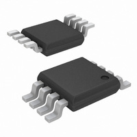
ISL21440IUZ-T13 Intersil, ISL21440IUZ-T13 Datasheet - Page 11

ISL21440IUZ-T13
Manufacturer Part Number
ISL21440IUZ-T13
Description
IC VREF W/COMPARATOR 8MSOP
Manufacturer
Intersil
Series
FGA™r
Datasheet
1.ISL21440IRTZ.pdf
(16 pages)
Specifications of ISL21440IUZ-T13
Applications
Comparator, Voltage Reference
Current - Supply
460µA
Voltage - Supply
2 V ~ 11 V
Operating Temperature
-40°C ~ 125°C
Mounting Type
Surface Mount
Package / Case
8-TSSOP, 8-MSOP (0.118", 3.00mm Width)
Lead Free Status / RoHS Status
Lead free / RoHS Compliant
Typical Performance Curves
Functional Description
Device Power
The ISL21440 device has a single positive supply pin, V+, and
two other supply pins, V- and GND. Normally for single supply
applications the V- pin is tied to system ground as well as the
GND pin. The separate ground pin allows the comparator to be
powered by split supplies from ±1.0V to ±5.5V. Note that the
minimum supply voltage will be 0.8V above the comparator
maximum input level for accurate operation.
Comparator Section
The comparator inputs can swing from the negative supply (GND
pin) to within 0.8V of the positive supply (V+). Alternatively, with
the comparator input set at the 1.182V reference level, the
minimum input voltage for accurate operation is 2.0V. If the
inputs are expected to see voltage levels above V+ or below
ground, they should be clamped with low leakage Schottky
diodes.
The CMOS output swings essentially from the GND potential to
V+ potential, depending on load current. If loads in excess of
FIGURE 23. OUTPUT RESPONSE TIME vs INPUT OVERDRIVE
270
245
220
195
170
145
120
95
70
45
20
10
5V
20
(t
3V
PLH
30
)
40
INPUT VOLTAGE (mV)
50
FIGURE 25. POWER-UP/DOWN OUTPUT RESPONSE (V+ = 3V, IN+ = V+, IN- = V
11
60
70
-0.5
3.5
3.0
2.5
2.0
1.5
1.0
0.5
80
0
0
90
0.2
100 110
0.4
(Continued)
0.6
ISL21440
120
0.8
TIME (ms)
1.0
1mA are expected, then a 0.1µF decoupling capacitor at the V+
pin should be added.
Voltage Reference Section
The voltage reference is a micropower FGA reference and is set
to 1.182V ±0.5% at the factory. The reference output can source
up to 2mA but the sink capability is very limited at only 10µA,
maximum. Small value capacitors, up to 10nF, can be used on
the reference output to lower noise if desired.
Applications Information
Handling and Board Mounting
FGA references provide excellent initial accuracy and low
temperature drift at the expense of very little power drain. There
are some precautions to take to insure this accuracy is not
compromised. Excessive heat during solder reflow can cause
excessive initial accuracy drift, so the recommended +260°C
max temperature profile should not be exceeded. Expect up to
1mV drift from the solder reflow process.
FGA references are susceptible to excessive X-radiation like that
used in PC board manufacturing. Initial accuracy can change
FIGURE 24. POWER-UP/DOWN OUTPUT RESPONSE
1.2
-0.5
5.5
5.0
4.5
4.0
3.5
3.0
2.5
2.0
1.5
1.0
0.5
OUT
0
0
1.4
0.2
1.6
(V+ = 5V, IN+ = V+, IN- = V
V+
0.4
1.8
0.6
2.0
0.8
REF
TIME (ms)
1.0
)
1.2
REF
OUT
)
1.4
February 23, 2011
1.6
V+
1.8
FN6532.2
2.0


