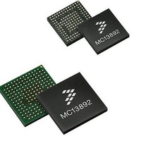
MC13892JVL Freescale Semiconductor, MC13892JVL Datasheet - Page 33

MC13892JVL
Manufacturer Part Number
MC13892JVL
Description
IC PMU I.MX51/37/35/27 186MAPBGA
Manufacturer
Freescale Semiconductor
Datasheets
1.MC13892AJVLR2.pdf
(156 pages)
2.MC13892AJVLR2.pdf
(2 pages)
3.MC13892AJVLR2.pdf
(16 pages)
4.MC13892JVL.pdf
(161 pages)
Specifications of MC13892JVL
Applications
Battery Management, Display (LED Drivers), Handheld/Mobile Devices, Power Supply
Operating Temperature
-40°C ~ 85°C
Mounting Type
Surface Mount
Package / Case
186-LFBGA
Output Current
65 mA
Output Voltage
1.5 V
Operating Temperature (max)
85C
Operating Temperature (min)
-40C
Mounting
Surface Mount
Package Type
BGA
Case Length
12mm
Screening Level
Industrial
Lead Free Status / RoHS Status
Lead free / RoHS Compliant
Current - Supply
-
Voltage - Supply
-
Lead Free Status / Rohs Status
Lead free / RoHS Compliant
Available stocks
Company
Part Number
Manufacturer
Quantity
Price
Company:
Part Number:
MC13892JVL
Manufacturer:
DALSA
Quantity:
4
Company:
Part Number:
MC13892JVL
Manufacturer:
Freescale Semiconductor
Quantity:
10 000
Part Number:
MC13892JVL
Manufacturer:
FREESCALE
Quantity:
20 000
Company:
Part Number:
MC13892JVLR2
Manufacturer:
Freescale Semiconductor
Quantity:
10 000
CFP AND CFM
capacitor connected between these pins to perform a first order filtering of the signal across R1.
CHRGSE1B
it can be left open since it is internally pulled up to VCORE. The recommendation is to place an external FET that can pull it low
or left it open, depending on the charge method.
CHRGLED
current sink is provided at the CHRGLED pin. This LED is to be connected between this pin and CHRGRAW.
GNDCHRG
LEDR, LEDG AND LEDB
These pins can also be used as general purpose open drain outputs for logic signaling, or as generic PWM generator outputs.
GNDLED
IC CORE
VCORE
bandgap and the rest of the core circuitry are supplied from VCORE. Place a 2.2 μF capacitor from this pin to GNDCORE.
VCOREDIG
powered as long as there is a valid supply and/or coin cell. Place a 2.2 μF capacitor from this pin to GNDCORE.
REFCORE
capacitor at REFCORE. No external DC loading is allowed on REFCORE. Place a 100 nF capacitor from this pin to GNDCORE.
GNDCORE
POWER GATING
PWGTDRV1 AND PWGTDRV2
and/or SW3. In addition, PWGTDRV2 provides support to power gate peripheral loads on the SW4 supply domain.
retained for the external memory in self refresh mode. SW1, SW2, and SW3 power gating FET drive would typically be connected
to PWGTDRV1 (for parallel NMOS switches). SW4 power gating FET drive would typically be connected to PWGTDRV2. When
low power Off mode is activated, the power gate drive circuitry will be disabled, turning off the NMOS power gate switches to
isolate the maintained supply domains from any peripheral loading.
Analog Integrated Circuit Device Data
Freescale Semiconductor
Accumulated current filter cap plus and minus terminals respectively. The coulomb counter will require a 10
An unregulated wall charger configuration can be built in which case this pin must be pulled low. When charging through USB,
Trickle LED driver output 1. Since normal LED control via the SPI bus is not always possible in the standalone operation, a
Ground for charger interface.
General purpose LED driver output Red, Green and Blue respectively. Each channel provides flexible LED intensity control.
Ground for LED drivers
Regulated supply output for the IC analog core circuitry. It is used to define the PUMS VIH level during initialization. The
Regulated supply output for the IC digital core circuitry. No external DC loading is allowed on VCOREDIG. VCOREDIG is kept
Main bandgap reference. All regulators use the main bandgap as the reference. The main bandgap is bypassed with a
Ground for the IC core circuitry.
Power Gate Drivers.
PWGTDRV1 is provided for power gating peripheral loads sharing the processor core supply domain(s) SW1, and/or SW2,
In typical applications, SW1, SW2, and SW3 will both be kept active for the processor modules in state retention, and SW4
FUNCTIONAL PIN DESCRIPTION
FUNCTIONAL DESCRIPTION
µ
F output
13892
33


