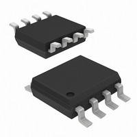
ADT7410TRZ Analog Devices Inc, ADT7410TRZ Datasheet - Page 18

ADT7410TRZ
Manufacturer Part Number
ADT7410TRZ
Description
IC SENSOR TEMP 16BIT I2C 8SOIC
Manufacturer
Analog Devices Inc
Specifications of ADT7410TRZ
Function
Temp Monitoring System (Sensor)
Topology
ADC (Sigma Delta), Oscillator, Register Bank
Sensor Type
Internal
Sensing Temperature
-55°C ~ 150°C
Output Type
I²C™
Output Alarm
No
Output Fan
No
Voltage - Supply
2.7 V ~ 5.5 V
Operating Temperature
-55°C ~ 150°C
Mounting Type
Surface Mount
Package / Case
8-SOIC (0.154", 3.90mm Width)
Ic Output Type
Digital
Sensing Accuracy Range
± 0.5°C
Supply Current
230µA
Supply Voltage Range
2.7V To 5.5V
Resolution (bits)
16bit
Sensor Case Style
SOIC
No. Of Pins
8
Lead Free Status / RoHS Status
Lead free / RoHS Compliant
For Use With
EVAL-ADT7X10EBZ - BOARD EVAL FOR ADT7410
Lead Free Status / RoHS Status
Lead free / RoHS Compliant, Lead free / RoHS Compliant
Available stocks
Company
Part Number
Manufacturer
Quantity
Price
Company:
Part Number:
ADT7410TRZ
Manufacturer:
ADI
Quantity:
620
Part Number:
ADT7410TRZ-REEL7
Manufacturer:
ADI/亚德诺
Quantity:
20 000
ADT7410
WRITING DATA
It is possible to write either a single byte of data or two bytes to
the ADT7410, depending on which registers are to be written.
Writing a single byte of data requires the serial bus address, the
data register address written to the address pointer register,
followed by the data byte written to the selected data register.
This is shown in Figure 15.
For the T
it is possible to write to both the MSB and the LSB registers in
SDA
SCL
SDA (CONTINUED)
SCL (CONTINUED)
START BY
MASTER
HIGH
SCL
SDA
START BY
MASTER
setpoint
1
1
, T
0
1
1
LOW
SERIAL BUS ADDRESS BYTE
D15
setpoint
1
0
0
SERIAL BUS ADDRESS BYTE
D14
FRAME 1
1
0
, and T
D13
0
FRAME 1
1
CRIT
Figure 15. Writing to a Register Followed by a Single Byte of Data
D12
Figure 16. Writing to a Register Followed by Two Bytes of Data
A1
SDA (CONTINUED)
SCL (CONTINUED)
0
setpoint
DATA BYTE
FRAME 3
D11
A0
A1
registers,
R/W
D10
A0
ADT7410
ACK. BY
D9
Rev. 0 | Page 18 of 24
9
R/W
ADT7410
ACK. BY
D8
P7
1
ADT7410
D7
ACK. BY
9
1
P6
9
D6
P7
1
the same write transaction. Writing two bytes of data to these
registers requires the serial bus address, the data register address
of the MSB register written to the address pointer register,
followed by the two data bytes written to the selected data
register. This is shown in Figure 16.
If more than the required number of data bytes is written to a
register, the register ignores these extra data bytes. To write to
a different register, a start or repeated start is required.
ADDRESS POINTER REGISTER BYTE
D7
P5
1
P6
D5
ADDRESS POINTER REGISTER BYTE
P4
D6
D4
P5
FRAME 2
DATA BYTE
FRAME 3
D5
P3
P4
D3
FRAME 2
P2
D4
P3
D2
DATA BYTE
FRAME 4
D3
P1
P2
D1
D2
P0
D0
P1
ADT7410
ACK. BY
ADT7410
ACK. BY
D1
9
P0
9
ADT7410
ACK. BY
D0
ADT7410
ACK. BY
9
STOP BY
MASTER
9
STOP BY
MASTER


