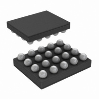
LP8720TLX-B/NOPB National Semiconductor, LP8720TLX-B/NOPB Datasheet - Page 12

LP8720TLX-B/NOPB
Manufacturer Part Number
LP8720TLX-B/NOPB
Description
IC REG BUCK 5-LDO I2C 20USMD
Manufacturer
National Semiconductor
Datasheet
1.LP8720TLENOPB.pdf
(24 pages)
Specifications of LP8720TLX-B/NOPB
Topology
Step-Down (Buck) Synchronous (1), Linear (LDO) (5)
Function
Any Function
Number Of Outputs
6
Frequency - Switching
2MHz
Voltage/current - Output 1
0.8 V ~ 2.3 V, 400mA
Voltage/current - Output 2
1.2 V ~ 3.3 V, 300mA
Voltage/current - Output 3
1.2 V ~ 3.3 V, 300mA
W/led Driver
No
W/supervisor
No
W/sequencer
Yes
Voltage - Supply
2.7 V ~ 4.5 V
Operating Temperature
-40°C ~ 85°C
Mounting Type
Surface Mount
Package / Case
20-UFBGA
Lead Free Status / RoHS Status
Lead free / RoHS Compliant
Available stocks
Company
Part Number
Manufacturer
Quantity
Price
Part Number:
LP8720TLX-B/NOPB
Manufacturer:
TI/德州仪器
Quantity:
20 000
www.national.com
I
I
I
I
I
I
I
I
I
V
V
Q(STANDBY)
Q(SLEEP)
Q(SLEEP)
Q(SLEEP)
Q(SLEEP)
Q
Q
Q
Q
POR_HI
POR_LO
Absolute Maximum Ratings
2)
If Military/Aerospace specified devices are required,
please contact the National Semiconductor Sales Office/
Distributors for availability and specifications.
Current Consumption
Unless otherwise noted, V
values and limits appearing in normal type apply for T
temperature range for operation, T
Power on Reset
Unless otherwise noted, V
values and limits appearing in normal type apply for T
temperature range for operation, T
V
VIN1, VIN2
All other pins
Junction Temperature (TJ-MAX)
Storage Temperature
Maximum Continuous Power
Dissipation
P
ESD
Symbol
Symbol
BATT
D-MAX
(Note
= VINB, VBATT
(Note
4)
Battery Standby Current
Battery Current in SLEEP
Mode @ 0 load
Battery Current in SLEEP
Mode @ 0 load
Battery Current in SLEEP
Mode @ 0 load
Battery Current in SLEEP
Mode @ 0 load
Battery Current @ 0 load
Battery Current @ 0 load
Battery Current @ 0 load
Battery Current @ 0 load
POR higher threshold
POR lower threshold
3)
Parameter
Parameter
VBATT
VBATT
-0.3V to V
-0.3V to V
=V
=V
VINB
VINB
J
J
= -40 to +125°C.
= -40 to +125°C.
=V
=V
BATT
BATT
VIN1
VIN1
V
BUCK and all LDO’s enabled
LDO1, LDO2, LDO3 and LDO4 enabled
LDO3 enabled
LDO1 and BUCK enabled
BUCK and all LDO’s enabled
LDO1, LDO2, LDO3 and LDO4 enabled
LDO3 enabled
LDO1 and BUCK enabled
V
V
BATT
VBATT
VBATT
+0.15V, max 6V
+0.3V, max 6V
=V
=V
(Note
-0.3V to +6V
-40 to 150ºC
VIN2
= 3.6V
VIN2
rising
falling
2 kV HBM
200V MM
=3.6V, GND=GNDB=0V, C
=3.6V, GND=GNDB=0V, C
1.75 W
(Note
(Note
1,
150ºC
J
J
=25°C. Limits appearing in boldface type apply over the entire junction
=25°C. Limits appearing in boldface type apply over the entire junction
Note
(Note
6)
Conditions
6)
Conditions
7)
12
Operating Ratings
Thermal Properties
V
VIN1, VIN2
All input-only pins
Junction Temperature (T
Ambient Temperature (T
Maximum Power Dissipation
Junction-to-Ambient Thermal Resistance (θ
(Jedec Standard Thermal PCB)
Micro SMD 20
BATT
= VINB, VBATT
(TA = 70ºC),
VBATT
VBATT
=C
=C
VIN1
VIN1
(Note
=C
=C
Typ
Typ
190
170
100
100
270
230
120
120
0.7
2.2
1.4
A
J
VIN2
VIN2
)
)
5)
=2.2 µF, C
=2.2 µF, C
(Note
Min
Min
(Note
2.0
1,
Limit
Limit
VINB
VINB
Note
9)
=10 µF. Typical
=10 µF. Typical
Max
Max
270
150
400
200
2.4
JA
2)
2.5V to V
5
-40 to 125ºC
)
0V to V
-40 to 85ºC
2.7 to 4.5V
45°C/W
1.2 W
Units
Units
BATT
BATT
µA
µA
µA
µA
µA
µA
µA
µA
µA
V
V


