EVAL-ADF4360-1EBZ1 Analog Devices Inc, EVAL-ADF4360-1EBZ1 Datasheet
EVAL-ADF4360-1EBZ1
Specifications of EVAL-ADF4360-1EBZ1
Q5594761


Related parts for EVAL-ADF4360-1EBZ1


EVAL-ADF4360-1EBZ1 Summary of contents
Page 1
FEATURES Output frequency range: 2050 MHz to 2450 MHz Divide-by-2 output 3 3.6 V power supply 1.8 V logic compatibility Integer-N synthesizer Programmable dual-modulus prescaler 8/9, 16/17, 32/33 Programmable output power level 3-wire serial interface Analog and digital ...
Page 2
ADF4360-1 TABLE OF CONTENTS Specifications..................................................................................... 3 Timing Characteristics..................................................................... 5 Absolute Maximum Ratings............................................................ 6 Transistor Count........................................................................... 6 ESD Caution.................................................................................. 6 Pin Configuration and Function Descriptions............................. 7 Typical Performance Characteristics ............................................. 8 Circuit Description........................................................................... 9 Reference Input Section............................................................... 9 Prescaler (P/P + ...
Page 3
SPECIFICATIONS 3.3 V ± 10%; AGND = DGND = VCO Table 1. Parameter REF CHARACTERISTICS IN REF Input Frequency IN REF Input Sensitivity IN REF Input Capacitance IN ...
Page 4
... REFIN PFD MHz MHz 2400; Loop B kHz. REFIN PFD 13 The spurious signals are measured with the EVAL-ADF4360-xEB1 Evaluation Board and the HP8562E Spectrum Analyzer. The spectrum analyzer provides the REF the synthesizer MHz @ 0 dBm. REFOUT B Version Unit −110 dBc/Hz typ −130 dBc/Hz typ − ...
Page 5
TIMING CHARACTERISTICS 3.3 V ± 10%; AGND = DGND = 0 V; 1.8 V and 3 V logic levels used VCO Table 2. Parameter Limit MIN MAX ...
Page 6
ADF4360-1 ABSOLUTE MAXIMUM RATINGS T = 25°C, unless otherwise noted. A Table 3. Parameter GND GND VCO VCO DD Digital I/O Voltage to GND Analog I/O ...
Page 7
PIN CONFIGURATION AND FUNCTION DESCRIPTIONS Table 4. Pin Function Descriptions Pin No. Mnemonic Description 1 CPGND Charge Pump Ground. This is the ground return path for the charge pump Analog Power Supply. This ranges from 3 ...
Page 8
ADF4360-1 TYPICAL PERFORMANCE CHARACTERISTICS 0 –10 –20 –30 –40 –50 –60 –70 1 –80 –90 2 –100 –110 –120 –130 –140 –150 –160 –170 1k 10k 100k FREQUENCY OFFSET (Hz) Figure 4. Open Loop VCO Phase Noise –70 –75 –80 ...
Page 9
CIRCUIT DESCRIPTION REFERENCE INPUT SECTION The reference input stage is shown in Figure 10. SW1 and SW2 are normally closed switches. SW3 is normally open. When power-down is initiated, SW3 is closed, and SW1 and SW2 are opened. This ensures ...
Page 10
ADF4360-1 MUXOUT AND LOCK DETECT The output multiplexer on the ADF4360 family allows the user to access various internal points on the chip. The state of MUXOUT is controlled by M3, M2, and M1 in the function latch. The full ...
Page 11
After band select, normal PLL action resumes. The nominal value MHz MHZ/V if divide-by-2 operation has been V selected (by programming DIV2 [DB22], high in the N counter latch). The ADF4360 family contains linearization ...
Page 12
ADF4360-1 LATCH STRUCTURE Table 6 shows the three on-chip latches for the ADF4360 family. The two LSBs determine which latch is programmed. Table 6. Latch Structure PRESCALER CURRENT VALUE SETTING 2 DB23 DB22 DB21 DB20 DB19 DB18 DB17 DB16 DB15 ...
Page 13
Table 7. Control Latch PRESCALER CURRENT VALUE SETTING 2 DB23 DB22 DB21 DB20 DB19 DB18 DB17 DB16 DB15 DB14 DB13 DB12 DB11 DB10 P2 P1 PD2 PD1 CPI6 CPI5 CPI4 CPI6 CPI5 CPI3 CPI2 ...
Page 14
ADF4360-1 Table 8. N Counter Latch DB23 DB22 DB21 DB20 DB19 DB18 DB17 DB16 DB15 DB14 DB13 DB12 DB11 DB10 DIV2 CPG B13 B12 B11 B10 DIVSEL B13 B12 B11 ...
Page 15
Table 9. R Counter Latch BAND BACKLASH SELECT CLOCK DB23 DB22 DB21 DB20 DB19 DB18 DB17 DB16 DB15 DB14 DB13 DB12 DB11 DB10 RSV RSV BSC2 BSC1 TMB LDP ABP2 TEST MODE BIT SHOULD BE SET TO 0 FOR NORMAL ...
Page 16
ADF4360-1 POWER-UP Power-Up Sequence The correct programming sequence for the ADF4360-1 after power-up is counter latch 2. Control latch 3. N counter latch Initial Power-Up Initial power-up refers to programming the part after the application of voltage to ...
Page 17
Hardware Power-Up/Power-Down If the ADF4360-1 is powered down via the hardware (using the CE pin) and powered up again without any change to the N counter register during power-down, it locks at the correct fre- quency because the part is ...
Page 18
ADF4360-1 CONTROL LATCH With (C2, C1) = (0, 0), the control latch is programmed. Table 7 shows the input data format for programming the control latch. Prescaler Value In the ADF4360 family, P2 and P1 in the control latch set ...
Page 19
N COUNTER LATCH With (C2, C1) = (1, 0), the N counter latch is programmed. Table 8 shows the input data format for programming the N counter latch. A Counter Latch program the 5-bit A counter. The ...
Page 20
ADF4360-1 APPLICATIONS DIRECT CONVERSION MODULATOR Direct conversion architectures are increasingly being used to implement base station transmitters. Figure 17 shows how ADI parts can be used to implement such a system. The circuit block diagram shows the AD9761 TxDAC® being ...
Page 21
FIXED FREQUENCY LO Figure 18 shows the ADF4360-1 used as a fixed frequency LO at 2.2 GHz. The low-pass filter was designed using ADIsimPLL for a channel spacing of 8 MHz and an open-loop bandwidth of 40 kHz. The maximum ...
Page 22
... ADF4360-1. Both single-ended architectures can be examined using the EVAL_ADF4360-1EB1 evaluation board. If the user does not need the differential outputs available on the ADF4360-1, the user may either terminate the unused out- put or combine both outputs using a balun ...
Page 23
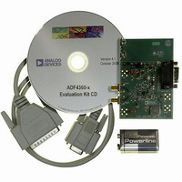
... MHz to 2450 MHz 2050 MHz to 2450 MHz 2050 MHz to 2450 MHz 2050 MHz to 2450 MHz Rev Page 0.60 MAX PIN 1 INDICATOR 2.45 EXPOSED 2.30 SQ PAD (BO TTOMVIEW) 2. 0.23 MIN 2.50 REF Package Option CP-24-2 CP-24-2 CP-24-2 CP-24-2 CP-24-2 CP-24-2 Evaluation Board ADF4360-1 ...
Page 24
ADF4360-1 NOTES 2 Purchase of licensed I C components of Analog Devices or one of its sublicensed Associated Companies conveys a license for the purchaser under the Philips I Rights to use these components system, ...