EVAL-ADF4360-3EBZ1 Analog Devices Inc, EVAL-ADF4360-3EBZ1 Datasheet - Page 16
EVAL-ADF4360-3EBZ1
Manufacturer Part Number
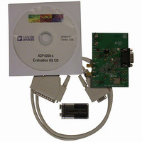
EVAL-ADF4360-3EBZ1
Description
BOARD EVALUATION FOR ADF4360-3
Manufacturer
Analog Devices Inc
Datasheet
1.ADF4360-3BCPZ.pdf
(24 pages)
Specifications of EVAL-ADF4360-3EBZ1
Main Purpose
Timing, Frequency Synthesizer
Embedded
No
Utilized Ic / Part
ADF4360-3
Primary Attributes
Single Integer-N PLL with VCO
Secondary Attributes
1.8GHz, 200kHz PFD
Lead Free Status / RoHS Status
Lead free / RoHS Compliant


ADF4360-3
POWER-UP
Power-Up Sequence
The correct programming sequence for the ADF4360-3 after
power-up is:
1.
2.
3.
Initial Power-Up
Initial power-up refers to programming the part after the
application of voltage to the AV
initial power-up, an interval is required between programming
the control latch and programming the N counter latch.
This interval is necessary to allow the transient behavior of the
ADF4360-3 during initial power-up to have settled. During
initial power-up, a write to the control latch powers up the part,
Table 10. C
C
10 µF
440 nF
N
Value
R counter latch
Control latch
N counter latch
N
Recommended Interval between Control Latch and N Counter latch
≥5 ms
≥600 µs
Capacitance vs. Interval and Phase Noise
POWER-UP
CLOCK
DATA
LE
DD
, DV
DD
LATCH DATA
R COUNTER
, V
VCO
, and CE pins. On
Figure 16. ADF4360-3 Power-Up Timing
LATCH DATA
Rev. B | Page 16 of 24
CONTROL
and the bias currents of the VCO begins to settle. If these cur-
rents have not settled to within 10% of their steady-state value,
and if the N counter latch is then programmed, the VCO may
not be able to oscillate at the desired frequency, which does not
allow the band select logic to choose the correct frequency
band, and the ADF4360-3 may not achieve lock. If the recom-
mended interval is inserted, and the N counter latch is pro-
grammed, the band select logic can choose the correct fre-
quency band, and the part locks to the correct frequency.
The duration of this interval is affected by the value of the ca-
pacitor on the C
the close-in noise of the ADF4360-3 VCO. The recommended
value of this capacitor is 10 µF. Using this value requires an in-
terval of ≥ 5 ms between the latching in of the control latch bits
and latching in of the N counter latch bits. If a shorter delay is
required, this capacitor can be reduced. A slight phase noise
penalty is incurred by this change, which is explained further
in Table 10.
CONTROL LATCH WRITE TO
N COUNTER LATCH WRITE
REQUIRED INTERVAL
N
pin (Pin 14). This capacitor is used to reduce
Open-Loop Phase Noise @ 10 kHz Offset
−87 dBc
−86 dBc
LATCH DATA
N COUNTER
Related parts for EVAL-ADF4360-3EBZ1
Image
Part Number
Description
Manufacturer
Datasheet
Request
R

Part Number:
Description:
±1.7g Dual-Axis IMEMS Accelerometer Evaluation Board
Manufacturer:
Analog Devices Inc
Datasheet:

Part Number:
Description:
Inertial Sensor Evaluation System
Manufacturer:
Analog Devices Inc
Datasheet:
Part Number:
Description:
Manufacturer:
Analog Devices Inc
Datasheet:
Part Number:
Description:
Manufacturer:
Analog Devices Inc
Datasheet:
Part Number:
Description:
Manufacturer:
Analog Devices Inc
Datasheet:
Part Number:
Description:
Manufacturer:
Analog Devices Inc
Datasheet:
Part Number:
Description:
Manufacturer:
Analog Devices Inc
Datasheet:
Part Number:
Description:
Manufacturer:
Analog Devices Inc
Datasheet:
Part Number:
Description:
Manufacturer:
Analog Devices Inc
Datasheet:
Part Number:
Description:
Manufacturer:
Analog Devices Inc
Datasheet:
Part Number:
Description:
Manufacturer:
Analog Devices Inc
Datasheet:
Part Number:
Description:
Manufacturer:
Analog Devices Inc
Datasheet:
Part Number:
Description:
Manufacturer:
Analog Devices Inc
Datasheet: